
SLIDE 1
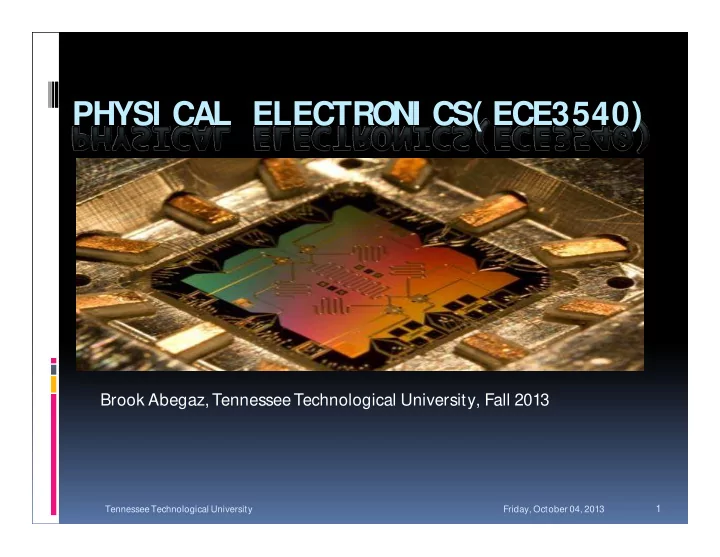
PHYSI CAL ELECTRO NI CS( ECE3540)
Brook Abegaz, Tennessee Technological University, Fall 2013
Friday, October 04, 2013 Tennessee Technological University
1
PHYSI CAL ELECTRO NI CS( ECE3540) Brook Abegaz, Tennessee - - PowerPoint PPT Presentation
PHYSI CAL ELECTRO NI CS( ECE3540) Brook Abegaz, Tennessee Technological University, Fall 2013 1 Tennessee Technological University Friday, October 04, 2013 C hapt er 1 The C r yst al St r uct ur e of Sol i ds Physical Electronics:
Brook Abegaz, Tennessee Technological University, Fall 2013
Friday, October 04, 2013 Tennessee Technological University
1
Friday, October 04, 2013 Tennessee Technological University
2
Friday, October 04, 2013 Tennessee Technological University
3
Friday, October 04, 2013 Tennessee Technological University
4
Friday, October 04, 2013 Tennessee Technological University
5
Material Resistivity
ρ (Ω* m) at 20 °C
Conductivity
σ (S/m) at 20 °C
Silver 1.59×10
−8
6.30×10
7
Copper 1.68×10
−8
5.96×10
7
Gold 2.44×10
−8
4.10×10
7
GaAs 5×10
−7 to 10×10 −3
5×10
−8 to 10
3
Germanium 4.6×10
−1
2.17 Silicon 6.40×10
2
1.56×10
−3
Glass 10×10
10 to 10×10 14
10
−11 to 10 −15
Air 1.3×10
16 to 3.3×10 16
3×10
−15 to 8×10 −15
Fused Quartz (SiO2) 7.5×10
17
1.3×10
−18
Teflon (C2F4)n 10×10
22 to 10×10 24
10
−25 to 10 −23
Friday, October 04, 2013 Tennessee Technological University
6
Friday, October 04, 2013 Tennessee Technological University
7
a) amorphous, b) polycrystalline, c) single crystalline
Friday, October 04, 2013 Tennessee Technological University
8
various possible unit cells.
Friday, October 04, 2013 Tennessee Technological University
9
Friday, October 04, 2013 Tennessee Technological University
10
Friday, October 04, 2013 Tennessee Technological University
11
.
.
Friday, October 04, 2013 Tennessee Technological University
12
Friday, October 04, 2013 Tennessee Technological University
13
Friday, October 04, 2013 Tennessee Technological University
14
Friday, October 04, 2013 Tennessee Technological University
15
Friday, October 04, 2013 Tennessee Technological University
16
Friday, October 04, 2013 Tennessee Technological University
17
Friday, October 04, 2013 Tennessee Technological University
18
Friday, October 04, 2013 Tennessee Technological University
19
Friday, October 04, 2013 Tennessee Technological University
20
Friday, October 04, 2013 Tennessee Technological University
21
Friday, October 04, 2013 Tennessee Technological University
22
Friday, October 04, 2013 Tennessee Technological University
23
Friday, October 04, 2013 Tennessee Technological University
24
Friday, October 04, 2013 Tennessee Technological University
25
Friday, October 04, 2013 Tennessee Technological University
26
Friday, October 04, 2013 Tennessee Technological University
27
Friday, October 04, 2013 Tennessee Technological University
28
Friday, October 04, 2013 Tennessee Technological University
29
Friday, October 04, 2013 Tennessee Technological University
30