
SLIDE 1
Monday, October 21, 2013 Tennessee Technological University
1
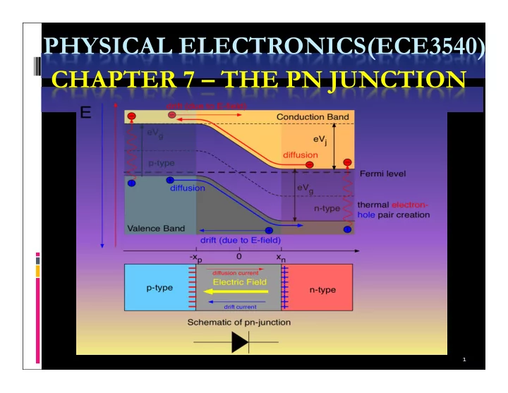
PHYSICAL ELECTRONICS(ECE3540) CHAPTER 7 – THE PN JUNCTION
Brook Abegaz
PHYSICAL ELECTRONICS(ECE3540) CHAPTER 7 THE PN JUNCTION 1 - - PowerPoint PPT Presentation
PHYSICAL ELECTRONICS(ECE3540) CHAPTER 7 THE PN JUNCTION 1 Tennessee Technological University Monday, October 21, 2013 Brook Abegaz The PN Junction Chapter 4 : we considered the semiconductor in equilibrium and determined electron and
Monday, October 21, 2013 Tennessee Technological University
1
Brook Abegaz
Monday, October 21, 2013 Tennessee Technological University
2
Monday, October 21, 2013 Tennessee Technological University
3
Monday, October 21, 2013 Tennessee Technological University
4
Monday, October 21, 2013 Tennessee Technological University
5
Monday, October 21, 2013 Tennessee Technological University
6
Monday, October 21, 2013 Tennessee Technological University
7
Monday, October 21, 2013 Tennessee Technological University
8
Monday, October 21, 2013 Tennessee Technological University
9
Monday, October 21, 2013 Tennessee Technological University
10
Monday, October 21, 2013 Tennessee Technological University
11
Monday, October 21, 2013 Tennessee Technological University
12
Monday, October 21, 2013 Tennessee Technological University
13
Fp Fn bi
F c c
Fi F i
Monday, October 21, 2013 Tennessee Technological University
14
F Fi Fn
Fn i
i d Fn
F Fi Fp
Fp i
i a Fp
2 2
i d a t i d a Fp Fn bi
Monday, October 21, 2013 Tennessee Technological University
15
Monday, October 21, 2013 Tennessee Technological University
16
Monday, October 21, 2013 Tennessee Technological University
17
d) Energy band Diagram
where (x) is the electric potential, E(x) is the electric field, (x) is the volume charge density, and ɛs is the permittivity of the semiconductor. The charge densities are:
Monday, October 21, 2013 Tennessee Technological University
18
s
2 2
n d p a
1 p s a s a s a s
1
n s d s d s d s
Monday, October 21, 2013 Tennessee Technological University
19
n d p a
2 2 2 n p s a n s d
2
p p s a
2 2 p a n d s n bi
Monday, October 21, 2013 Tennessee Technological University
20
a n d p
2 1
d a d a bi s n
2 1
d a a d bi s p
2 1
d a d a bi s
Monday, October 21, 2013 Tennessee Technological University
21
2 2
i d a t i d a Fp Fn bi
Monday, October 21, 2013 Tennessee Technological University
22
2
i d a t bi
For Nd = 1015cm‐3 Vbi(V) Na = 1015cm‐3 0.575V Na = 1016cm‐3 0.635 Na = 1017cm‐3 0.695 Na = 1018cm‐3 0.754 For Nd = 1018cm‐3 Vbi(V) Na = 1015cm‐3 0.754V Na = 1016cm‐3 0.814 Na = 1017cm‐3 0.874 Na = 1018cm‐3 0.933
Monday, October 21, 2013 Tennessee Technological University
23
2 2
i d a t i d a Fp Fn bi
2 1
d a d a bi s
Monday, October 21, 2013 Tennessee Technological University
24
Fi F
10 16
F Fi
10 16
i d a t bi
2 10 16 16 2
Monday, October 21, 2013 Tennessee Technological University
25
2 1 16 16 16 16 19 14
n d 4 14 4 16 19 max
p n
Monday, October 21, 2013 Tennessee Technological University
26
R Fp Fn total
R bi total
Monday, October 21, 2013 Tennessee Technological University
27
Monday, October 21, 2013 Tennessee Technological University
28
Monday, October 21, 2013 Tennessee Technological University
29
2 1
d a d a R bi s
2 1 max
d a d a s R bi
R bi
max
Monday, October 21, 2013 Tennessee Technological University
30
p a n d
' R
' '
Monday, October 21, 2013 Tennessee Technological University
31
R n d R
' ' 2 1
d a d a R bi s n
2 1 '
d a R bi d a s
Monday, October 21, 2013 Tennessee Technological University
32
2 1
d a d a R bi s
2 1 '
d a R bi d a s
s
'
Monday, October 21, 2013 Tennessee Technological University
33
2 1
d a d a R bi s
2 2
i d a t i d a Fp Fn bi
Monday, October 21, 2013 Tennessee Technological University
34
2 1
d a d a R bi s
2 1 15 16 15 16 19 14
Monday, October 21, 2013 Tennessee Technological University
35
Monday, October 21, 2013 Tennessee Technological University
36
a d
Monday, October 21, 2013 Tennessee Technological University
37 Impurity Concentration Surface X = X’ Nd Na
Monday, October 21, 2013 Tennessee Technological University
38 X = 0
X0 +
N-region
Monday, October 21, 2013 Tennessee Technological University
39
s s
2 2
s s
barrier for this function. Another expression for the built-in potential barrier is:
potential barrier Vbi + VR. Solving for x0 and using the total potential barrier, we obtain:
as we used for the uniformly doped junction. The junction capacitance is then:
Monday, October 21, 2013 Tennessee Technological University
40
bi s s s
3 3 2 3
2 0 )
i t bi
3 1
R bi s
3 1 2 '
} ) ( 12 {
R bi s
V V ea C
Monday, October 21, 2013 Tennessee Technological University
41 dx0 dx0 X = 0
X0 +
N-region
(C/cm3) +dQ’=(x0)dx0 = eax0dx0
reverse-bias voltage for a linearly graded PN Junction. Note that C' is proportional to (Vbi + VR)-1/3 for the linearly graded junction as compared to C'(Vbi + VR)-1/2 for the uniformly doped junction. In the linearly graded junction, the capacitance is less dependent on reverse-bias voltage than in the uniformly doped junction.
Monday, October 21, 2013 Tennessee Technological University
42
m
Monday, October 21, 2013 Tennessee Technological University
43 Bx0
m
m=+3 m=-1 m=+2 m=+1 m=-2 m=-3 N-type doping profiles x=0 x0 m=0
is given as: when m is negative, the capacitance becomes a very strong function of reverse-bias voltage, a desired characteristic in Varacter diodes. The term Varactor comes from the words variable reactor and means a device whose reactance can be varied in a controlled manner with bias voltage.
LC circuit and the capacitance of the diode can be written in the form:
linear function of reverse-bias voltage VR so we need:
Monday, October 21, 2013 Tennessee Technological University
44
) 2 ( 1 ) 1 ( '
m R bi m s
) 2 ( 1
m R bi
2
http://ecee.colorado.edu/~bart/book/book/contents.htm
http://www.doitpoms.ac.uk/tlplib/semiconductors/pn.php
http://wanda.fiu.edu/teaching/courses/Modern_lab_manual/pn_junction.html
Monday, October 21, 2013 Tennessee Technological University
45