PHYSICAL ELECTRONICS(ECE3540) CHAPTER 8 THE PN JUNCTION DIODE - - PowerPoint PPT Presentation

physical electronics ece3540
SMART_READER_LITE
LIVE PREVIEW

PHYSICAL ELECTRONICS(ECE3540) CHAPTER 8 THE PN JUNCTION DIODE - - PowerPoint PPT Presentation

PHYSICAL ELECTRONICS(ECE3540) CHAPTER 8 THE PN JUNCTION DIODE CHAPTER 8 THE PN JUNCTION DIODE 1 Tennessee Technological University Wednesday, October 23, 2013 Brook Abegaz The PN Junction Diode Chapter 4 : we considered the


slide-1
SLIDE 1

Wednesday, October 23, 2013 Tennessee Technological University

1

PHYSICAL ELECTRONICS(ECE3540)

CHAPTER 8 –THE PN JUNCTION DIODE CHAPTER 8 –THE PN JUNCTION DIODE

Brook Abegaz

slide-2
SLIDE 2

The PN Junction Diode

  • Chapter 4: we considered the semiconductor in

equilibrium and determined electron and hole concentrations in the conduction and valence bands, respectively.

  • The net flow of

the electrons and holes in a semiconductor generates current. The process by which these charged particles move is called transport.

  • Chapter 5: we considered the two basic transport

mechanisms in a semiconductor crystal: drift: the movement of charge due to electric fields, and diffusion: the flow of charge due to density gradients.

Wednesday, October 23, 2013 Tennessee Technological University

2

slide-3
SLIDE 3

The PN Junction Diode

  • Chapter 6: we discussed the behavior of non-

equilibrium electron and hole concentrations as functions of time and space.

  • We developed the ambi-polar transport equation

which describes the behavior of the excess electrons and holes.

  • Chapter 7: We considered the situation in which a

p-type and an n-type semiconductor are brought into contact with one another to form a PN junction.

Wednesday, October 23, 2013 Tennessee Technological University

3

slide-4
SLIDE 4

The PN Junction Diode

  • Previous

Chapters:

we have been considering the properties of the semiconductor material by calculating electron and hole concentrations in thermal equilibrium and determined the position of the Fermi level.

  • Previous Chapter: We considered the non-

equilibrium condition in which excess electrons and holes are present in the semiconductor.

  • We discussed the electrostatics of the PN junction in

thermal equilibrium and under reverse bias.

  • We determined the built-in potential barrier in thermal

equilibrium and calculated the electric field in the space charge region. We also considered the junction capacitance.

Wednesday, October 23, 2013 Tennessee Technological University

4

slide-5
SLIDE 5

The PN Junction Diode

  • Chapter 8: We will consider the PN junction with a

forward-bias voltage applied and will determine the current-voltage characteristics. The potential barrier of the PN junction is lowered when a forward bias voltage is applied, allowing electrons and holes to flow across the space charge region.

  • When holes flow from the p region across the space

charge region into the n region, they become excess minority carrier holes and are subject to excess minority carrier diffusion, drift, and recombination.

  • Likewise, when electrons from the n region flow

across the space charge region into the p region, they become excess minority carrier electrons and are subject to these same processes.

Wednesday, October 23, 2013 Tennessee Technological University

5

slide-6
SLIDE 6

The PN Junction Diode

  • When a sufficiently large reverse-bias voltage is applied

across a PN junction, breakdown can occur, producing a large reverse-bias current in the junction, which can cause heating effects and catastrophic failure of the diode.

  • Zener diodes, however, are designed to operate in the

breakdown region. Breakdown puts limits on the amount

  • f voltage that can be applied across a PN junction.
  • When a forward-bias voltage is applied to a PN junction,

a current will be induced in the device. We initially consider a qualitative discussion of how charges flow in the PN junction and then consider the mathematical derivation of the current-voltage relationship.

Wednesday, October 23, 2013 Tennessee Technological University

6

slide-7
SLIDE 7

Reverse and Forward Applied Bias

Wednesday, October 23, 2013 Tennessee Technological University

7

  • Fig. 8.1: Energy band diagram of a PN Junction under reverse and forward bias
slide-8
SLIDE 8

Qualitative Description of Charge Flow in a PN Junction

  • We can qualitatively understand the mechanism of the current in a

PN Junction by considering the energy band diagrams. In the last chapter, we argued that the potential barrier seen by the electrons holds back the large concentration of electrons/holes in the n/p region and keeps them from flowing into the p/n region. The potential barrier, then, maintains thermal equilibrium.

  • The potential of the n region is positive with respect to the p

region so the Fermi energy in the n region is lower than that in the p region. The total potential barrier is now larger than for the zero- bias case. We argued in the last chapter that the increased potential barrier continues to hold back the electrons and holes so that there is still essentially no charge flow and hence essentially no current.

Wednesday, October 23, 2013 Tennessee Technological University

8

slide-9
SLIDE 9

Qualitative Description of Charge Flow in a PN Junction

  • When a positive voltage is applied to the p region with respect to

the n region, the Fermi level in the p region is lowered than that in the n region. The total potential barrier is now reduced. The smaller potential barrier means that the electric field in the depletion region is also reduced.

  • The smaller electric field means that the electrons and holes are no

longer held back in the n and p regions, respectively. There will be a diffusion of holes from the p region across the space-charge region where they now will flow into the n region. Similarly, there will be a diffusion of electrons from the n region across the space- charge region where they will flow into the p region. The flow of charge generates current through the PN junction.

Wednesday, October 23, 2013 Tennessee Technological University

9

slide-10
SLIDE 10

The PN Junction Current

  • The injection of holes into the n region means that these

holes are minority carriers. Likewise, the injection of electrons into the p-region means that these electrons are minority carriers.

  • The behavior of these minority carriers is described by

the ambi-polar transport equations that were discussed in Chapter 6. There will be diffusion as well as recombination of excess carriers in these regions. The diffusion of carriers implies that there will be diffusion currents.

  • The mathematical derivation of the PN junction current-

voltage relationship is considered in the next slides.

Wednesday, October 23, 2013 Tennessee Technological University

10

slide-11
SLIDE 11

Ideal Current-Voltage Relationships

  • The ideal current-voltage relationship of a PN junction is derived

based

  • n

four assumptions. The abrupt depletion layer approximation applies. The space charge regions have abrupt boundaries and the semiconductor is neutral outside of the depletion region.

  • 1. The Maxwell-Boltzmann approximation applies to carrier statistics.
  • 2. The concept of low injection applies.
  • 3. The concept of total and individual currents:

a) The total current is a constant throughout the entire PN

structure.

b) The individual electron and hole currents are continuous

functions through the PN structure.

c) The

individual electron and hole currents are constant throughout the depletion region.

Wednesday, October 23, 2013 Tennessee Technological University

11

slide-12
SLIDE 12

Boundary Conditions

  • Considering the conduction-band energy through the PN junction in thermal

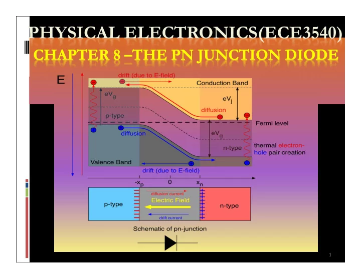
equilibrium, the region contains many more electrons in the conduction band than the p region; the built-in potential barrier prevents this large density of electrons from flowing into the p region. The built-in potential barrier maintains equilibrium between the carrier distributions on either side of the junction.

  • An expression for the built-in potential barrier was derived in the last chapter

and was given as:

  • If we divide the equation by Vt = kT/e, take the exponential of both sides, and

then take the reciprocal, we obtain (assuming complete ionization):

  • where nn0 is the thermal-equilibrium concentration of majority carrier electrons

in the n region.

Wednesday, October 23, 2013 Tennessee Technological University

12

                   

2 2

ln ln | | | |

i d a t i d a Fp Fn bi

n N N V n N N e kT V           kT eV N N n

bi d a i

exp

2 d n

N n 

slide-13
SLIDE 13

Boundary Conditions

  • In the p region, we can write:
  • where np0 is the thermal-equilibrium concentration of minority carrier electrons.

Substitution yields:

  • This equation relates the minority carrier electron concentration on the p side
  • f the junction to the majority carrier electron concentration on the n side of

the junction in thermal equilibrium.

  • If a positive voltage is applied to the p region with respect to the n region, the

potential barrier is reduced.

  • The electric field in the bulk p and n regions is normally very small. Essentially

all of the applied voltage is across the junction region. The electric field Eapp induced by the applied voltage is in the opposite direction to the thermal equilibrium space charge electric field, so the net electric field in the space charge region is reduced below the equilibrium value.

Wednesday, October 23, 2013 Tennessee Technological University

13

a i p

N n n

2 0 

        kT eV n n

bi n p

exp

slide-14
SLIDE 14

The PN Junction Current

  • Under applied potential, the electric field force that prevented majority carriers

from crossing the space charge region is reduced; majority carrier electrons/holes from the n/p side are injected across the depletion region into the p/n material.

  • As long as the bias Va is applied, the injection of carriers across the space charge

region continues and a current is created in the PN junction. This bias condition is known as forward bias.

  • The potential barrier Vbi can be replaced by (Vbi -Va) when the junction is forward

biased.

  • If we assume low injection, the majority carrier electron concentration nn0 does

not change significantly. However, the minority carrier concentration np can deviate from its thermal-equilibrium value np0 by orders of magnitude.

Wednesday, October 23, 2013 Tennessee Technological University

14

                       kT eV kT eV n kT V V e n n

a bi n a bi n p

exp exp ) ( exp        kT eV n n

a p p

exp         kT eV n n

bi n p

exp

slide-15
SLIDE 15

The PN Junction Current

  • When a forward-bias voltage is applied to the PN junction, the junction is no

longer in thermal equilibrium. The total minority carrier electron concentration in the p region is now greater than the thermal equilibrium value. The forward- bias voltage lowers the potential barrier so that majority carrier electrons from the n region are injected across the junction into the p region, thereby increasing the minority carrier electron concentration. We have produced excess minority carrier electrons in the p region.

  • When the electrons/holes are injected into the p/n region, these excess carriers

are subject to the diffusion and recombination processes. We can write that:

  • where pn0 is the concentration of minority carrier holes at the edge of the space

charge region in the n region.

  • By applying a forward-bias voltage, we create excess minority carriers in each

region of the PN junction.

Wednesday, October 23, 2013 Tennessee Technological University

15

       kT eV p p

a n n

exp         kT eV p p

bi p n

exp

slide-16
SLIDE 16

Exercise

  • 1. Consider a Silicon PN junction at T = 300 K

so that ni = 1.5 x 1010 cm-3. Assume the n-type doping is 1 x 1016 cm-3 and assume that a forward bias of 0.60 V is applied to the PN

  • Junction. Calculate the minority carrier hole

concentration at the edge of the space charge region for the forward bias that is applied.

Wednesday, October 23, 2013 Tennessee Technological University

16

       kT eV p p

a n n

exp

slide-17
SLIDE 17

Solution

1.

From the equation:

  • The thermal-equilibrium minority carrier hole concentration is
  • We then have
  • Comment: The minority carrier concentration can increase by

many orders of magnitude when a forward bias voltage is

  • applied. Low injection still applies; however, since the excess-

electron concentration (equal to the excess-hole concentration in order to maintain charge neutrality) is much less than the thermal-equilibrium electron concentration.

Wednesday, October 23, 2013 Tennessee Technological University

17

3 4 16 2 2 2

10 25 . 2 10 ) 10 5 . 1 (

   cm x x N n p

d i n 3 14 4

10 59 . 2 0259 . 60 . exp 10 25 . 2

        cm x x p n        kT eV p p

a n n

exp

slide-18
SLIDE 18

The PN Junction Current

  • The minority carrier concentrations at the space charge

edges were derived assuming a forward-bias voltage (Va>0) was applied across the pn junction. However, same analysis could be applied for Va being negative (reverse bias).

  • If a reverse-bias voltage greater than a few tenths of a volt

is applied to the PN junction, then we see from that the minority carrier concentrations at the space charge edge are essentially zero.

  • The minority carrier concentrations for the reverse-bias

condition drop below the thermal equilibrium values.

Wednesday, October 23, 2013 Tennessee Technological University

18

slide-19
SLIDE 19

Minority Carrier Distribution

  • The ambi-polar transport equation for excess minority carrier holes in an n region

is:

  • where pn = pn – pn0 is the excess minority carrier hole concentration and is the

difference between the total and thermal equilibrium minority carrier concentrations.

  • As a first approximation, we will assume that the electric field is zero in both the

neutral p and n regions. In the n region for x > xn we have that E = 0 and g' = 0. If we also assume steady state so (pn)/ (t) = 0, then:

  • For the same set of conditions, the excess minority carrier electron concentration

in the p region is determined from:

Wednesday, October 23, 2013 Tennessee Technological University

19

t p p g x p E x p D

n p n n p n p

          ) ( ) ( ) (

' 2 2

      ) ( : ) (

2 2 2 n p n n

x x L p x p       

2 p p p

D L  

) ( : ) (

2 2 2 p n p p

x x L n x n       

2 n n n

D L  

slide-20
SLIDE 20

Minority Carrier Distribution

  • The

boundary conditions for the total minority carrier concentrations are:

Wednesday, October 23, 2013 Tennessee Technological University

20

       kT eV p x p

a n n n

exp ) (         kT eV n x n

a p p p

exp ) ( ) (

n n

p x p     ) (

p p

n x n    

slide-21
SLIDE 21

Minority Carrier Distribution

  • As minority carriers diffuse from the space charge edge into the neutral

semiconductor regions, they will recombine with majority carriers. The excess minority carrier concentrations must approach zero at distances far from the space charge region. The structure is referred to as a long PN junction.

  • The general solution is:
  • Applying the boundary conditions, the coefficients A and D must be zero. The

coefficients B and C may be determined from the boundary conditions. The excess carrier concentrations are then found to be:

Wednesday, October 23, 2013 Tennessee Technological University

21

) ( : ) ( ) (

n L x L x n n n

x x Be Ae p x p x p

p p

    

 ) ( : ) ( ) (

p L x L x p p p

x x De Ce n x n x n

n n

     

 ) exp( ] 1 ) [exp( ) ( ) (

p n a n n n n

L x x kT eV p p x p x p       ) exp( ] 1 ) [exp( ) ( ) (

n p a p p p p

L x x kT eV n n x n x n      

slide-22
SLIDE 22

Minority Carrier Distribution

  • The minority carrier concentrations decay exponentially with

distance away from the junction to their thermal-equilibrium

  • values. Again, we have assumed that both the n-region and the p-

region lengths are long compared to the minority carrier diffusion lengths.

  • To review, a forward-bias voltage lowers the built-in potential

barrier of a PN junction so that electrons from the n region are injected across the space charge region, creating excess minority carriers in the p region. These excess electrons begin diffusing into the bulk p region where they can recombine with majority carrier holes.

  • The excess minority carrier electron concentration then decreases

with distance from the junction. The same discussion applies to holes injected across the space charge region into the n region.

Wednesday, October 23, 2013 Tennessee Technological University

22

slide-23
SLIDE 23

Ideal PN Junction Current

  • The total current in the junction is the sum of the individual electron and

hole currents which are constant through the depletion region.

  • Since the electron and hole currents are continuous functions through

the PN junction, the total PN junction current will be the minority carrier hole diffusion current at x = xn plus the minority carrier electron diffusion current at x = -xp.

  • The gradients in the minority carrier concentrations produce diffusion

currents, and since we are assuming the electric field to be zero at the space charge edges, we can neglect any minority carrier drift current component.

  • We can calculate the minority carrier hole diffusion current density as:
  • (assuming uniformly doped regions)

Wednesday, October 23, 2013 Tennessee Technological University

23

n

x x n p n p

dx x p d eD x J

  | )) ( ( ) ( 

n

x x n p n p

dx x dp eD x J

  | ) ( ) (

slide-24
SLIDE 24

Ideal PN Junction Current

  • Taking the derivative and substituting: :
  • The hole current density for this forward-bias condition is in the +x

direction, which is from the p to the n region.

  • Similarly, we may calculate the electron diffusion current density at x=-xp.

This may be written as:

  • Using Equation (8.15). we obtain:
  • The electron current density is also in the +x direction.
  • An assumption we made at the beginning was that the individual electron

and hole currents were continuous functions and constant through the space charge region. The total current is the sum of the electron and hole currents and is constant through the entire junction.

Wednesday, October 23, 2013 Tennessee Technological University

24

] 1 ) [exp( ) (   kT eV L p eD x J

a p n p n p

p

x x p n p n

dx x n d eD x J

 

  | )) ( ( ) ( 

] 1 ) [exp( ) (    kT eV L n eD x J

a n p n p n

slide-25
SLIDE 25

Ideal PN Junction Current

  • The total current density in the PN junction is then:
  • Parameter Js is defined as:
  • Substituting Js, the ideal diode equation may be written as:

Wednesday, October 23, 2013 Tennessee Technological University

25

] 1 ) [exp( ) ( ) (               kT eV L n eD L p eD x J x J J

a n p n p n p p n n p

         

n p n p n p s

L n eD L p eD J ] 1 ) [exp( ) ( ) (      kT eV J x J x J J

a s p n n p

slide-26
SLIDE 26

Ideal PN Junction Current

  • The above equation, known as the ideal-diode equation, gives a

good description of the current-voltage characteristics of the PN junction over a wide range of currents and voltages. Although the equation was derived assuming a forward-bias voltage, there is nothing to prevent Va from being negative (reverse bias).

  • If the voltage Va becomes negative (reverse bias) by a few kT/e V,

then the reverse-bias current density becomes independent of the reverse-bias voltage. The parameter Js is then referred to as the reverse saturation current density. The current-voltage characteristics of the PN junction diode are obviously not bilateral.

Wednesday, October 23, 2013 Tennessee Technological University

26

] 1 ) [exp( ) ( ) (      kT eV J x J x J J

a s p n n p

slide-27
SLIDE 27

Reverse and Forward Applied Bias

Wednesday, October 23, 2013 Tennessee Technological University

27

  • Fig. 8.2: Ideal I-V Characteristic of a PN Junction Diode
slide-28
SLIDE 28

Exercise

  • 2. Consider the following parameters in a Silicon

PN Junction:

 Na = Nd = 1016cm-3

ni = 1.5 x 1010 cm-3

 Dn= 25 cm2/s

p0= n0 = 5 x10⁻⁷ s

 Dp = 10 cm2/s

r = 11.7

  • Determine the ideal reverse saturation current

density in the Silicon PN junction at T = 100 K.

Wednesday, October 23, 2013 Tennessee Technological University

28

slide-29
SLIDE 29

Solution

  • 2. The ideal reverse saturation current density is given by

which may be rewritten as: Substituting the parameters, we obtain Js = 4.15x10⁻¹¹A/cm2

  • Comment
  • The ideal reverse-bias saturation current density is very
  • small. If the PN Junction cross-sectional area were A =

10-4 cm2, for example, then the ideal reverse-bias diode current would be Is = 4.15 x 10⁻¹⁵ A.

Wednesday, October 23, 2013 Tennessee Technological University

29

         

n p n p n p s

L n eD L p eD J          

2

1 1

p d d n n a i s

D N D N en J  

slide-30
SLIDE 30

Total Forward Bias Current

  • The total forward-bias current density in the PN junction is the

sum of the recombination and the ideal diffusion current densities.

  • The diode current-voltage relationship can be written as:
  • where n is called the ideality factor and 1<n<2.
  • For a large forward-bias voltage, n=1 when diffusion dominates and for low

forward-bias, n=2 when recombination dominates.

Wednesday, October 23, 2013 Tennessee Technological University

30

] 1 ) [exp(   nkT eV I I

a s D rec

J J J                 kT eV J kT eV eWn J

a r a i rec

2 exp 2 exp 2         kT eV J J

a s D

exp

slide-31
SLIDE 31

Reading Assignment

  • Please read the concepts of Junction Breakdown and the
  • peration principles of Zener Diodes from your text

book (last pages of Chapter 8).

  • In class, we have started explaining these concepts.
  • After the reading assignment, we will go through the

concepts of a large reverse-bias voltage that causes a Junction Breakdown.

  • We will also discuss the Zener Effect and the Avalanche

Effect.

Wednesday, October 23, 2013 Tennessee Technological University

31

slide-32
SLIDE 32

Picture Credits

  • Semiconductor Physics and Devices, Donald Neaman, 4th

Edition, McGraw Hill Publications.

  • B. Van Zeghbroeck, Principles of

Electronic Devices, Department

  • f

ECE, University

  • f

Colorado, Boulder, 2011.

http://ecee.colorado.edu/~bart/book/book/contents.htm

  • Animation of the PN Junction formation, University
  • f Cambridge, 2013.

http://www.doitpoms.ac.uk/tlplib/semiconductors/pn.php

  • W. U. Boeglin, PN Junction, Florida International

University, 2011.

http://wanda.fiu.edu/teaching/courses/Modern_lab_manual/pn_junction.html

Wednesday, October 23, 2013 Tennessee Technological University

32