PHYSICAL ELECTRONICS(ECE3540) CHAPTER 6 CARRIER GENERATION AND - - PowerPoint PPT Presentation

physical electronics ece3540
SMART_READER_LITE
LIVE PREVIEW

PHYSICAL ELECTRONICS(ECE3540) CHAPTER 6 CARRIER GENERATION AND - - PowerPoint PPT Presentation

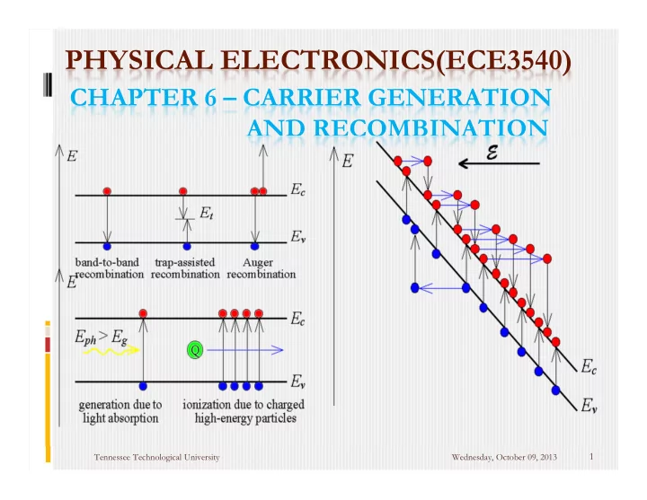
PHYSICAL ELECTRONICS(ECE3540) CHAPTER 6 CARRIER GENERATION AND RECOMBINATION 1 Tennessee Technological University Wednesday, October 09, 2013 Chapter 6 Carrier Generation and Recombination Chapter 4 : we considered the


slide-1
SLIDE 1

PHYSICAL ELECTRONICS(ECE3540)

Wednesday, October 09, 2013 Tennessee Technological University

1

CHAPTER 6 – CARRIER GENERATION AND RECOMBINATION

slide-2
SLIDE 2

Chapter 6 – Carrier Generation and Recombination

  • Chapter 4: we considered the semiconductor

in equilibrium and determined electron and hole concentrations in the conduction and valence bands, respectively.

  • The net flow of the electrons and holes in a

semiconductor will generate currents. The process by which these charged particles move is called transport.

  • Chapter 5: we considered the two basic transport

mechanisms in a semiconductor crystal: drift the movement of charge due to electric fields, and diffusion the flow of charge due to density gradients.

Wednesday, October 09, 2013 Tennessee Technological University

2

slide-3
SLIDE 3

Chapter 6 – Carrier Generation and Recombination

  • Chapter 6: we will discuss the behavior of

non-equilibrium electron and hole concentrations as functions of time and space.

  • We

will develop the ambi-polar transport equation which describes the behavior of the excess electrons and holes.

  • We can define two new parameters that apply to

the non-equilibrium semiconductor: the quasi- Fermi energy for electrons and the quasi-Fermi energy for holes.

Wednesday, October 09, 2013 Tennessee Technological University

3

slide-4
SLIDE 4

Carrier Generation and Recombination

  • Generation: is the process whereby electrons and holes

are created.

  • Recombination: is the process whereby electrons and

holes are annihilated.

  • Any deviation from thermal equilibrium will tend to

change the electron and hole concentrations in a semiconductor.

  • Examples:

 A sudden increase in temperature will increase the rate at which

electrons and holes are thermally generated so that their concentrations will change with time until new equilibrium values are reached.

 An external excitation, such as light (a flux of photons), can also

generate electrons and holes, creating a non-equilibrium condition.

Wednesday, October 09, 2013 Tennessee Technological University

4

slide-5
SLIDE 5

The Semiconductor in Equilibrium

  • Since

the net carrier concentrations are independent of time in thermal equilibrium, the rate at which electrons and holes are generated and the rate at which they recombine must be equal.

  • Let Gn0 and Gp0 be the thermal-generation rate
  • f electrons and holes in #/cm3-s. For a direct

band-to-band generation, the electrons and holes are created in pairs, therefore: Gn0 = Gp0.

Wednesday, October 09, 2013 Tennessee Technological University

5

slide-6
SLIDE 6

The Semiconductor in Equilibrium

Wednesday, October 09, 2013 Tennessee Technological University

6

  • Let Rn0 and Rp0 be the recombination rates of electrons

and holes, respectively, for a semiconductor in thermal equilibrium, again given in units of #/cm3-s.

  • In direct band-to-band recombination, electrons and

holes recombine in pairs, so that Rn0 = Rp0.

  • In thermal equilibrium, the concentrations of electrons

and holes are independent of time; therefore, the generation and recombination rates are equal, so we have Gn0 = Gp0 = Rn0 = Rp0

  • Fig. 6.1: Electron-hole generation and recombination
  • +

+

  • Electron-Hole

Generation Electron-Hole Recombination X

slide-7
SLIDE 7

Excess Carrier Generation and Recombination

  • Electrons in the valence band may be excited into the

conduction band when, for example, high-energy photons are incident on a semiconductor.

  • When this happens, not only is an electron created in

the conduction band, but a hole is created in the valence band; thus an electron-hole pair is generated.

  • The additional electrons and holes created are called

excess electrons and excess holes.

Wednesday, October 09, 2013 Tennessee Technological University

7

slide-8
SLIDE 8

Excess Carrier Generation and Recombination

  • The excess electrons and holes are generated by an

external force at a particular rate.

  • Let gn’ be the generation rate of excess electrons and gp’

be the generation rate of excess holes in units of #/cm3s

  • For the direct band-to-band generation, the excess

electrons and holes are also created in pairs, so we must have gn’ = gp’.

  • When excess electrons and holes are created, the

concentration of electrons in the conduction band and

  • f holes in the valence band increase above their thermal

equilibrium value.

  • We may write n = n0 + n and p = p0 + p. n0 and p0 are

the thermal-equilibrium concentrations, and n and p are the excess electron and hole concentrations.

Wednesday, October 09, 2013 Tennessee Technological University

8

slide-9
SLIDE 9

Excess Carrier Generation and Recombination

Wednesday, October 09, 2013 Tennessee Technological University

9

Symbol Definition no, po Thermal equilibrium electron and hole concentration (independent of time and position) n, p Total electron and hole concentrations (may be functions of time and/or position) n = n – n0 Excess electron concentration (may be function of time and/or position) p = p – p0 Excess hole concentration (may be function of time and/or position) gn’ , gp’ Excess electron and hole generation rates. Rn’ , Rp’ Excess electron and hole recombination rates. n0, p0 Excess minority carrier electron and hole lifetimes.

  • Table. 6.1: Notations used in Carrier Generation and Recombination
slide-10
SLIDE 10

Excess Carrier Generation and Recombination

  • A steady-state generation of excess electrons and holes will not cause

a continual buildup of the carrier concentrations. As in the case of thermal equilibrium, an electron in the conduction band may "fall down" into the valence band, leading to the process of excess electron-hole recombination.

  • The recombination rate for excess electrons is denoted by Rn’, and for

excess holes by Rp’.

  • Both parameters have units of #/cm3-s. The excess electrons and

holes recombine in pairs, so the recombination rates must be equal. We can then write Rn’ = Rp’.

  • In the direct band-to-band recombination that we are considering, the

recombination occurs spontaneously: thus, the probability of an electron and hole recombining is constant with time.

  • The rate at which electrons recombine must be proportional to the

electron concentration and must also be proportional to the hole concentration.

  • If there are no electrons or holes, there can be no recombination.

Wednesday, October 09, 2013 Tennessee Technological University

10

slide-11
SLIDE 11

Excess Carrier Generation and Recombination

  • The net rate of change in the electron concentration can

be written as:

(eq. 6.1) where

  • rni

2 (eq. 6.1) is thermal-equilibrium generation rate.

  • Since excess

electrons and holes are created and recombine in pairs, n(t) = p(t). (Excess electron and hole concentrations are equal and termed excess carriers.)

  • The

thermal-equilibrium parameters, n0 and p0, independent of time, become: (eq. 6.2)

Wednesday, October 09, 2013 Tennessee Technological University

11

)] ( ) ( [ ) (

2

t p t n n dt t dn

i r

   ) ( ) ( t n n t n    ) ( ) ( t p p t p    )] ( ) )[( ( ))] ( ))( ( ( [ )) ( (

2

t n p n t n t p p t n n n dt t n d

r i r

              

slide-12
SLIDE 12

Excess Carrier Generation and Recombination

  • (Eq. 6.2) can easily be solved if we impose the condition of

Low Level Injection.

  • In an extrinsic n-type material, we generally have no >> po

and, in an extrinsic p-type material, we generally have po >>no.

  • Low-level

injection means that the excess carrier concentration is much less than the thermal equilibrium majority carrier concentration.

  • Conversely, high-level injection occurs when the excess

carrier concentration becomes comparable to or greater than the thermal equilibrium majority carrier concentrations.

  • If we consider a p-type material (po >> no) under low-level

injection (n(t) <<po), then (eq. (6.2)) is: (eq. (6.2)

Wednesday, October 09, 2013 Tennessee Technological University

12

) ( )) ( ( t n p dt t n d

r

    

slide-13
SLIDE 13

Excess Carrier Generation and Recombination

  • The solution to the equation is an exponential decay

from the initial excess concentration, or (eq. 6.3)

where n0 = (rp0)-1 and is a constant for the low-level injection.

  • The above equation describes the decay of excess

minority carrier electrons so that n0 is often referred to as the excess minority carrier lifetime.

Wednesday, October 09, 2013 Tennessee Technological University

13

/

) ( ) ( ) (

n r

t t p

e n e n t n

 

  

 

 

slide-14
SLIDE 14

Excess Carrier Generation and Recombination

  • The recombination rate defined as a positive quantity--of excess minority carrier

electrons can be written as:

  • For the direct band-to-band recombination, the excess majority carrier holes

recombine at the same rate, so that for the p-type material

  • For an n-type material (n0 >> p0) under low-level injection (n(t) <<no), the decay
  • f minority carrier holes occurs with a time constant p0= (rno)-1 where p0 is also

referred to as the excess minority carrier lifetime. The recombination rate of the majority carrier electrons is the same as that of the minority carrier holes, so we have

  • The generation rates of excess carriers are not functions of electron or hole
  • concentrations. In general, the generation and recombination rates may be

functions of the space coordinates and time.

Wednesday, October 09, 2013 Tennessee Technological University

14

'

)) ( ( ) ( )) ( (

n r n

t n t n p dt t n d R          

' '

) (

n p n

t n R R    

' '

) (

p p n

t p R R    

slide-15
SLIDE 15

Exercise

  • 1. Consider a semiconductor in which n0 = 1013

cm-3 and ni = 1010 cm-3. Assume that the excess-carrier lifetime is 10-6 s. Determine the electron-hole recombination rate if the excess- hole concentration is p = 5 x 1013 cm-3.

Wednesday, October 09, 2013 Tennessee Technological University

15

' '

) (

p p n

t p R R    

slide-16
SLIDE 16

Solution

  • 1. n-type semiconductor, low-injection so that

Wednesday, October 09, 2013 Tennessee Technological University

16

1 3 19 6 13

10 5 10 10 5 '

  

   s cm x x p R

p

 

slide-17
SLIDE 17

Exercise

  • 2. A semiconductor in thermal equilibrium, has a

hole concentration of p0= 1016 cm-3 and an intrinsic concentration of ni = 1010 cm-3. The minority carrier lifetime is 2 x 10⁷ s.

(a) Determine the thermal-equilibrium recombination rate of electrons. (b) Determine the change in the recombination rate of electrons if an excess electron concentration of n = 1012 cm-3 exists.

Wednesday, October 09, 2013 Tennessee Technological University

17

' '

) (

n p n

t n R R    

slide-18
SLIDE 18

Solution

a) thermal-equilibrium recombination rate of

electrons and Then

Wednesday, October 09, 2013 Tennessee Technological University

18

n n

n R  

3 4 16 2 10 2

10 10 ) 10 (

   cm p n n

i 1 3 10 7 4

10 5 ) 10 2 ( ) 10 (

  

  s cm x x Rn

slide-19
SLIDE 19

Solution

b) the

change in the recombination rate

  • f

electrons if an excess electron concentration of n = 1012 cm-3 exists Therefore,

Wednesday, October 09, 2013 Tennessee Technological University

19

1 3 18 7 12

10 5 10 2 10

   

  s cm x x n R

n n

 

10 18

10 5 10 5 x x R R R

n n n

    

1 3 18

10 5

 

  s cm x Rn

slide-20
SLIDE 20

Continuity Equations

  • The continuity equations for electrons and holes are

shown as a differential volume element in which a

  • ne-dimensional hole particle flux is entering the

differential element at r and is leaving at x + dx.

  • The parameter Fpx

+ is the hole-particle flux, or flow,

and has units of number of holes/cm2-s.

  • For the x component of the particle current density:

Wednesday, October 09, 2013 Tennessee Technological University

20

dx x F x F dx x F

px px px

. ) ( ) (     

  

  • Fig. 6.2: Differential volume showing x component of the hole-particle flux.

Fpx

+(x)

Fpx

+(x+dx)

x x+dx dy dz

slide-21
SLIDE 21

Continuity Equations

  • This equation is a Taylor expansion of Fpx

+(x + dx).

where the differential length dx is small, so that only the first two terms in the expansion are significant. The net increase in the number of holes per unit time within the differential volume element due to the x- component of hole flux is given by:

  • If Fpx

+(x) > Fpx + (x + dx), for example, there will be

a net increase in the number of holes in the differential volume element with time.

Wednesday, October 09, 2013 Tennessee Technological University

21

dxdydz x F dydz dx x F x F dxdydz t p

px px px

        

  

)] ( ) ( [

slide-22
SLIDE 22

Continuity Equations

  • The generation rate and recombination rate of holes will also affect

the hole concentration in the differential volume. The net increase in the number of holes per unit time in the differential volume element is then given by

where p is the density of holes.

  • The first term on the right side of the equation is the increase in the

number of holes per unit time due to the hole flux, the second term is the increase in the number of holes per unit time due to the generation of holes, and the last term is the decrease in the number

  • f holes per unit time due to the recombination of holes.
  • The recombination rate for holes is given by p/pt

where pt includes the thermal equilibrium carrier lifetime and the excess carrier lifetime.

Wednesday, October 09, 2013 Tennessee Technological University

22

dxdydz P dxdydz g dxdydz x F dxdydz t p

pt p px

        

slide-23
SLIDE 23

Continuity Equations

  • If we divide both sides of the equation by the differential

volume dx.dy.dz, the net increase in the hole concentration per unit time is :

  • The above equation is known as the continuity equation

for holes.

  • Similarly, the one-dimensional continuity equation for

electrons is given by:

where Fn

  • is the electron-particle flow, or flux, also given in units
  • f number of electrons/cm2-s.

Wednesday, October 09, 2013 Tennessee Technological University

23

pl p p

p g x F t p         

 nl n n

n g x F t n         

slide-24
SLIDE 24

Time-Dependent Diffusion Equations

  • The hole and electron current densities are given as:
  • Dividing the hole current density by (+e) and the

electron current density by (-e) to find the flux of each particle:

Wednesday, October 09, 2013 Tennessee Technological University

24

x p eD pE e J

p p p

     x n eD nE e J

n n n

     x p D pE F e J

p p p p

     

 ) ( x n D nE F e J

n n n n

     

 ) (

slide-25
SLIDE 25

Time-Dependent Diffusion Equations

  • Taking

the divergence

  • f

the equations, and substituting back into the continuity equations:

  • Keeping in mind that we are limiting ourselves to a
  • ne-dimensional

analysis, we can expand the derivative of the product as

Wednesday, October 09, 2013 Tennessee Technological University

25

pt p p p

p g x p D x pE t p             

2 2

) (

nt n n n

n g x n D x nE t n             

2 2

) ( x E p x p E x pE         ) (

slide-26
SLIDE 26

Time-Dependent Diffusion Equations

  • In a more generalized three-dimensional analysis, the

above equation would have to be replaced by a vector identity.

  • The above equations are the time-dependent diffusion

equations for holes and electrons, respectively. Since both the hole concentration p and the electron concentration n contain the excess concentrations, the equations describe the space and time behavior of the excess carriers.

Wednesday, October 09, 2013 Tennessee Technological University

26

t p p g x E p x p E x p D

pt p p p

               ) ) ( ) ( (

2 2

t n n g x E n x n E x n D

pt n n n

               ) ) ( ) ( (

2 2

slide-27
SLIDE 27

Time-Dependent Diffusion Equations

  • The hole and electron concentrations are functions of

both the thermal equilibrium. The thermal equilibrium concentrations, no and po. are not functions of time.

  • For the special case of a homogeneous semiconductor,

no and po are also independent of the space coordinates, therefore:

  • Note that the Equations (6.29) and (6.30) contain terms

involving the total concentrations, p and n, and terms involving only the excess concentrations, p and n.

Wednesday, October 09, 2013 Tennessee Technological University

27

t p p g x E p x p E x p D

pt p p p

             ) ( ) ) ( ) ( ( ) (

2 2

     t n n g x E n x n E x n D

pt n n n

             ) ( ) ) ( ) ( ( ) (

2 2

    

slide-28
SLIDE 28

Ambipolar Transport

  • If a pulse of excess electrons and a pulse of excess holes are

created at a particular point in a semiconductor with an applied electric field, the excess holes and electrons will tend to drift in opposite directions.

  • Electrons and holes are charged particles, any separation will

induce an internal electric field between the two sets of

  • particles. This internal electric field will create a force

attracting the electrons and holes back toward each other.

  • The electric field is then composed of the externally applied

field plus the induced internal field.

Wednesday, October 09, 2013 Tennessee Technological University

28

int

E E E

app 

Eapp app n x

  • +

+ +

  • Fig. 6.3: The creation of an internal electric field

as excess electrons and holes tend to separate.

slide-29
SLIDE 29

Ambipolar Transport

  • Since the internal E-field creates a force attracting the

electrons and holes, this E-field will hold the pulses

  • f excess electrons and excess holes together.
  • The negatively charged electrons and positively

charged holes then will drift or diffuse together with a single effective mobility or diffusion coefficient.

  • This phenomenon is called ambipolar diffusion or

ambipolar transport:

Wednesday, October 09, 2013 Tennessee Technological University

29

t n R g x n E x n D           ) ( ) ( ) (

' 2 2 '

   

slide-30
SLIDE 30

Ambipolar Transport

Wednesday, October 09, 2013 Tennessee Technological University

30

t n R g x n E x n D           ) ( ) ( ) (

' 2 2 '

    p n n p

p n p n

        ) (

'

p D n D p n D D D

p n p n

   ) (

'

The ambipolar diffusion coefficient D’ and the ambipolar mobility coefficient μ’ are defined from Einstein’s relation as follows: Applications of Ambipolar Transport: Illustration of the behavior

  • f excess carriers in semiconductors, in PN junction diodes and other

devices.

slide-31
SLIDE 31

Exercise

  • 3. Consider an infinitely large, homogeneous n-

type semiconductor with a zero applied electric field. Assume that, for t < 0, the semiconductor is in thermal equilibrium and that, for t≥0, a uniform generation rate exists in the crystal.

 Calculate the excess carrier concentration as a

function of time assuming the condition of low injection (where excess carrier concentration is much lower than thermal equilibrium majority carrier concentration n<<p0 (p type) or p<<n0 (n type) )

Wednesday, October 09, 2013 Tennessee Technological University

31

t n R g x n E x n D           ) ( ) ( ) (

' 2 2 '

   

slide-32
SLIDE 32

Solution

  • The condition of a uniform generation rate and a

homogeneous semiconductor implies that:

  • Therefore, the ambipolar transport equation

reduces to:

  • The solution of the differential is:

Wednesday, October 09, 2013 Tennessee Technological University

32

) ( ) (

2 2

      x p x p   t p p g

p

    ) (

'

   ) 1 ( ) (

'

p

t p

e g t p

 

  t p R g x p E x p D           ) ( ) ( ) (

' 2 2 '

   

slide-33
SLIDE 33

Exercise

  • 4. Consider an n-type Silicon at T = 300K doped

at Nd = 2 x 1016cm-3. Assume that p0 = 10-7s and g' = 5 x 1021 cm-3s-l. Determine the time dependence of excess carriers in reaching a steady-state condition. Does low injection apply?

Wednesday, October 09, 2013 Tennessee Technological University

33

) 1 ( ) (

'

p

t p

e g t p

 

 

slide-34
SLIDE 34

Solution

  • 4. Using the equation:
  • Therefore,

Note 1: for t  ∞, the steady state excess hole and electron concentration of 5x1014cm-3 exists. Note 2: p<<n0 therefore low injection is valid.

Wednesday, October 09, 2013 Tennessee Technological University

34

) 1 ( ) (

'

p

t p

e g t p

 

 

3 10 14 10 7 21

] 1 [ 10 5 ) 1 )( 10 ( ) 10 5 ( ) (

7 7

   

 

     cm e x e x t p

t t

slide-35
SLIDE 35

Dielectric Relaxation Time Constant

Wednesday, October 09, 2013 Tennessee Technological University

35

  • Quasi-neutrality condition: the concentration of excess holes is

balanced by an equal concentration of excess electrons.

  • If a uniform concentration of holes p is suddenly injected into a

portion of the surface of a semiconductor, we will instantly have a concentration of excess holes and a net positive charge density that is not balanced by a concentration of excess electrons. How is charge neutrality achieved and how fast?

  • Dielectric Relaxation Time Constant

N type p holes

  • Fig. 6.4: The injection of a concentration of holes into a

small region at the surface of an n-type semiconductor

slide-36
SLIDE 36

Dielectric Relaxation Time Constant

  • There are three defining equations to be considered.
  • Poisson's equation is: (gradient of electric field equals net

charge density divided by permittivity)

  • From Ohm’s Law : (current density equals conductivity

times electric field)

  • And from continuity equation, neglecting the effects of

generation and recombination:

  • The parameter  is the net charge density and the initial

value is given by e(p). We will assume that p is uniform over a short distance at the surface. The parameter  is the permittivity of the semiconductor.

Wednesday, October 09, 2013 Tennessee Technological University

36

    E . E J   t J       .

slide-37
SLIDE 37

Dielectric Relaxation Time Constant

  • Taking the divergence of Ohm's law and using

Poisson's equation:

  • Substituting the above equation into the continuity

equation,

which can be rearranged into the first order equation: Whose solution is: Dielectric Relaxation Time Constant is:

Wednesday, October 09, 2013 Tennessee Technological University

37

       E J . . dt d t          

            dt d

d

t

e t

 

 ) ( ) (    

d

slide-38
SLIDE 38

Exercise

  • 5. Assume an n-type Silicon semiconductor with a

donor impurity concentration of Nd =1016cm-3 and mobility n = 1200cm2/V.sec .

  • Calculate the dielectric relaxation time constant.

Wednesday, October 09, 2013 Tennessee Technological University

38

slide-39
SLIDE 39

Solution

  • 5. The conductivity is found as
  • The permittivity of Silicon is calculated as:

The dielectric relaxation time constant is then:

Wednesday, October 09, 2013 Tennessee Technological University

39

1 16 19

) ( 92 . 1 ) 10 )( 1200 )( 10 * 6 . 1 (

 

    cm N e

d n

  cm F

r

/ ) 10 * 85 . 8 )( 7 . 11 (

14 

     s cm cm F

d 13 1 14

10 * 39 . 5 ) 92 . 1 ( / ) 10 * 85 . 8 )( 7 . 11 (

  

   

slide-40
SLIDE 40

Picture Credits

  • Semiconductor Physics and Devices, Donald Neaman, 4th

Edition, McGraw Hill Publications.

  • B. Van Zeghbroeck, Principles of Semiconductor Devices,
  • Dept. of ECE, University of Colorado, Boulder, 2011

http://ecee.colorado.edu/~bart/book/book/toc2.htm

Wednesday, October 09, 2013 Tennessee Technological University

40