
SLIDE 1
Hybrid single nanowire y g photonic crystal structures
Hong Gyu Park Hong-Gyu Park
- Dept. of Physics, Korea University
Hybrid single nanowire y g photonic crystal structures Hong Gyu - - PowerPoint PPT Presentation
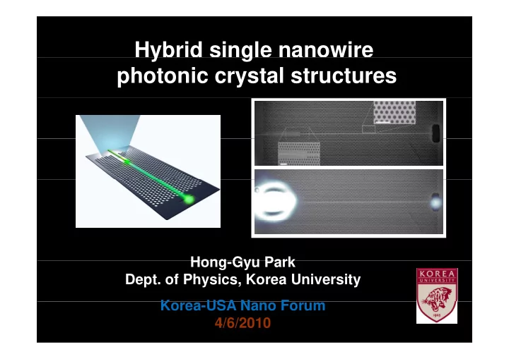
Hybrid single nanowire y g photonic crystal structures Hong Gyu Park Hong-Gyu Park Dept. of Physics, Korea University K Korea-USA Nano Forum USA N F 4/6/2010 Semiconductor Nanowire for Photonics Semiconductor nanowires as building
Scanning Electron Microscope image
10nm 5
Transmission Electron Microscope image Mi h t l i
10nm
5 μm
Micro-photoluminescence
10nm
C.J. Barrelet, Y. Wu, D. C. Bell, C. M. Lieber, J A Ch S 125 11498 (2003)
SEM images
Photoluminescence images (below & above threshold)
200nm 200nm
Photoluminescence spectrum & L-L curve
2μm
Lasing spectrum
p
http://ab-initio.mit.edu/photons/tutorial/
defect/cavity
VCSEL (Bell Lab) Self-organized assembly (UK) Periodic air holes (KAIST)
defect/cavity
H G Park et al Science 305 1444 (2004)
H.-G. Park et al., Science 305, 1444 (2004).
(Schematics)
(SEM image of fabricated structure)
C.J. Barrelet, J. Bao, M. Loncar, H.-G. Park, F. Capasso, C.M. Lieber, Nano Lett. 6, 11 (2006).
SEM f th CdS i f i th t i ht id SEM of the CdS nanowire facing the straight waveguide
waveguide
d = 80nm l = ~5μm
5 microns
Photoluminescence superimposed on the SEM image l = ~5μm
5 microns
(PL spectra)
input
5 microns
(PL spectra)
input
H.-G. Park, C.J. Barrelet, Y. Wu, B. Tian, F. Qian, C.M. Lieber, Nature Photonics 2, 622 (2008).