
SLIDE 1
1
The Spartan 3e FPGA
CS/EE 3710
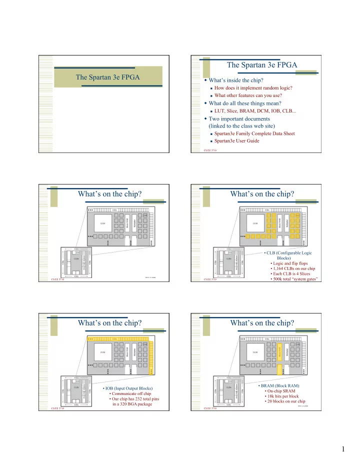
The Spartan 3e FPGA
What’s inside the chip?
How does it implement random logic? What other features can you use?
What do all these things mean?
LUT, Slice, BRAM, DCM, IOB, CLB...
Two important documents (linked to the class web site)
Spartan3e Family Complete Data Sheet Spartan3e User Guide CS/EE 3710
What’s on the chip?
CS/EE 3710
What’s on the chip?
- CLB (Configurable Logic
Blocks)
- Logic and flip flops
- 1,164 CLBs on our chip
- Each CLB is 4 Slices
- 500k total “system gates”
CS/EE 3710
What’s on the chip?
- IOB (Input Output Blocks)
- Communicate off chip
- Our chip has 232 total pins
in a 320 BGA package
CS/EE 3710
What’s on the chip?
- BRAM (Block RAM)
- On-chip SRAM
- 18k bits per block
- 20 blocks on our chip