
SLIDE 1
Digital Systems Clock Distribution I CMPE 650 1 (5/1/07)
UMBC
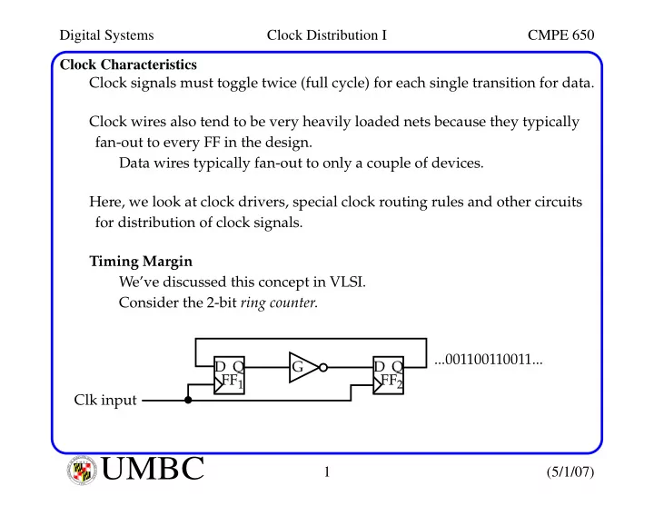
U M B C U N I V E R S I T Y O F M A R Y L A N D B A L T I M O R E C O U N T Y 1 9 6 6Clock Characteristics Clock signals must toggle twice (full cycle) for each single transition for data. Clock wires also tend to be very heavily loaded nets because they typically fan-out to every FF in the design. Data wires typically fan-out to only a couple of devices. Here, we look at clock drivers, special clock routing rules and other circuits for distribution of clock signals. Timing Margin We’ve discussed this concept in VLSI. Consider the 2-bit ring counter. Clk input D Q D Q G ...001100110011... FF2 FF1