WWW.FPGA What is an FPGA? Field Programmable Gate Array - - PowerPoint PPT Presentation

fpga
SMART_READER_LITE
LIVE PREVIEW

WWW.FPGA What is an FPGA? Field Programmable Gate Array - - PowerPoint PPT Presentation

WWW.FPGA What is an FPGA? Field Programmable Gate Array Introduction to FPGA designs Generic logic cells + Programmable switches Why do we use it? High performance & Flexible Shorter time to market Joachim Rodrigues


slide-1
SLIDE 1

Joachim Rodrigues, EIT, LTH, Introduction to Structured VLSI Design jrs@eit.lth.se FPGA Intro

Introduction to FPGA designs

Joachim Rodrigues‐Chenxin Zhang Department of Electrical and Information Technology Lund University, Sweden

Joachim Rodrigues, EIT, LTH, Introduction to Structured VLSI Design jrs@eit.lth.se FPGA Intro

WWW.FPGA

  • What is an FPGA?

– Field Programmable Gate Array – Generic logic cells + Programmable switches

  • Why do we use it?

– High performance & Flexible – Shorter time to market

  • Where do we use it?

– Digital signal processing – ASIC prototyping – Software‐defined radio – Medical imaging – Computer vision …

Joachim Rodrigues, EIT, LTH, Introduction to Structured VLSI Design jrs@eit.lth.se FPGA Intro

FPGA vs. Microprocessor

Intel Itanium 2 Xilinx Virtex-II Pro (XC2VP100) Technology 0.13 µm 0.13 µm Clock speed 1.6 GHz 180 MHz Internal memory bandwidth 102 GBytes/S 7.5 TBytes/S #Processing units 5 FPU (2 MACs + 1 FPU) 6 MMU 6 Integer units 212 FPU or 300+ Integer units or … Power consumption 130 W 15 W Peak performance 8 GFLOPs 38 GFLOPs Sustained performance ~2GFLOPs ~19 GFLOPs IO/External memory bandwidth 6.4 GBytes/S 67 GBytes/S

Joachim Rodrigues, EIT, LTH, Introduction to Structured VLSI Design jrs@eit.lth.se FPGA Intro

FPGA devices

  • Major manufactures

– Xilinx: Spartan, Virtex – Altera: Cyclone, Arria, Stratix – Lattice Semiconductor – Actel – Atmel …

  • We use Xilinx Spartan‐3 board in this course!

http://www.digilentinc.com/Products/Detail.cfm?NavPath=2,400,519&Prod=S3BOARD

slide-2
SLIDE 2

Joachim Rodrigues, EIT, LTH, Introduction to Structured VLSI Design jrs@eit.lth.se FPGA Intro

  • A RAM‐based architecture

– Configurable Logic Blocks (CLBs) – Programmable switches – Input/Output Blocks (IOBs)

Xilinx Spartan‐3 FPGAs (I)

LUT-based logic cell

Joachim Rodrigues, EIT, LTH, Introduction to Structured VLSI Design jrs@eit.lth.se FPGA Intro

Xilinx Spartan‐3 FPGAs (II)

  • XC3S200:

– 480 CLBs = 480*4 Slices = 480*4*2*(4‐input LUTs + registers) – 12 18‐kbit dual‐port BRAMs = 12*18 Kb = 216 Kbits – 12 18‐bit dedicated multipliers – 4 Digital Clock Managers (DCMs) – 173 User I/Os

Joachim Rodrigues, EIT, LTH, Introduction to Structured VLSI Design jrs@eit.lth.se FPGA Intro

Xilinx Spartan‐3 FPGAs (III)

Each slice contains 2 LUT-based logic cells and 4 slices form a CLB

Joachim Rodrigues, EIT, LTH, Introduction to Structured VLSI Design jrs@eit.lth.se FPGA Intro

Xilinx Spartan‐3 FPGAs (IV)

  • Example: 2‐bit adder (s = a + b)

b1 a1 b0 a0 s1 s0

1 1 1 1 1 1 1 1 1

1 1 1 1 1 1 1 1 1 1 1 1 1 1 1 1 1 1 1 1 1 1 1 1 1 1 1 1 1 1 1 1 1 1 1 1 1 1 1

s1 s0

Carry generation Sum generation

slide-3
SLIDE 3

Joachim Rodrigues, EIT, LTH, Introduction to Structured VLSI Design jrs@eit.lth.se FPGA Intro

FPGA Clocking resources

Joachim Rodrigues, EIT, LTH, Introduction to Structured VLSI Design jrs@eit.lth.se FPGA Intro

Clock Non‐Idealities

  • Clock skew

– Spatial variation in temporally equivalent clock edges. – Skew is a time offset of the clocks. It is a fixed difference between technically identical clocks caused by intra‐device clock network, device process variations, and unbalanced loading.

  • Clock jitter

– Temporal variations in consecutive edges of the clock signal – Jitter occurs due to system noise and signal crosstalk and causes phase uncertainty resulting in ambiguity in the rising and falling edge

  • f a signal.

– Jitter can be both random and deterministic.

Joachim Rodrigues, EIT, LTH, Introduction to Structured VLSI Design jrs@eit.lth.se FPGA Intro

Clock Non‐Idealities

  • Both skew and jitter affects the cycle time
  • Skew might lead to race through the registers

tskew tjitter

Same clock at two different locations of the chip

Joachim Rodrigues, EIT, LTH, Introduction to Structured VLSI Design jrs@eit.lth.se FPGA Intro

Clock Skew

  • Absolute Skew

‐Delay from input to leaf cell

  • Relative Skew

‐Delay difference between leaf cells Too much clock skew may: 1) Force you to reduce clock rate 2) Cause malfunction at any clock rate

slide-4
SLIDE 4

Joachim Rodrigues, EIT, LTH, Introduction to Structured VLSI Design jrs@eit.lth.se FPGA Intro

Distributed Buffers in H-tree

Small relative skew Absolute skew of less importance

Clock

Joachim Rodrigues, EIT, LTH, Introduction to Structured VLSI Design jrs@eit.lth.se FPGA Intro

Synthesized Clock tree

Clock buffers are placed in the core row gaps

Clock tree in an ASIC

Joachim Rodrigues, EIT, LTH, Introduction to Structured VLSI Design jrs@eit.lth.se FPGA Intro

Spartan‐III‐ Clocking resources

  • Each global clock multiplexer buffer can be driven either by the clock pad

to distribute a clock directly to the device, or by the Digital Clock Manager (DCM)

  • Eight global clocks can be used in each quadrant of the Virtex‐II Pro

device.

Joachim Rodrigues, EIT, LTH, Introduction to Structured VLSI Design jrs@eit.lth.se FPGA Intro

Spartan III‐ Clocking resources

  • 16 Global Clock inputs (GCLK0

through GCLK15)

  • 8 Right-Half Clock inputs (RHCLK0

through RHCLK7)

  • 8 Left-Half Clock inputs (LHCLK0

through LHCLK7)

  • Clock input pins are used

automatically when external signals drive clock buffers

slide-5
SLIDE 5

Joachim Rodrigues, EIT, LTH, Introduction to Structured VLSI Design jrs@eit.lth.se FPGA Intro

Spartan III‐ Global clock

  • IBUFG is inferred by the

synthesis tool on any top‐ level clock port.

  • Global clocks are driven by

dedicated clock buffers (IBUFG), which can also be used to

– gate the clock (BUFGCE) – multiplex between two independent clock inputs (BUFGMUX).

Joachim Rodrigues, EIT, LTH, Introduction to Structured VLSI Design jrs@eit.lth.se FPGA Intro

Clock‐buffer‐ VHDL

BUFG_inst : BUFG port map ( O => O, -- Clock buffer output I => I -- Clock buffer input );

  • - End of BUFG_inst

instantiation BUFG_inst : BUFG port map ( O => O, -- Clock buffer output I => I -- Clock buffer input );

  • - End of BUFG_inst

instantiation BUFGCE_1_inst : BUFGCE_1 port map ( O => O, -- Clock buffer ouptput CE => CE, -- Clock enable input I => I -- Clock buffer input );

  • - End of BUFGCE_1_inst instantiation

BUFGCE_1_inst : BUFGCE_1 port map ( O => O, -- Clock buffer ouptput CE => CE, -- Clock enable input I => I -- Clock buffer input );

  • - End of BUFGCE_1_inst instantiation

Joachim Rodrigues, EIT, LTH, Introduction to Structured VLSI Design jrs@eit.lth.se FPGA Intro

Digital Clock Manager (DCM)

  • Spartan III accommodates 4

DCM’s

  • DCM introduces phase shift, clock

division/multiplication

  • Can be instantiated by direct

instantiation, or Coregen

  • Skew less clock distribution

Joachim Rodrigues, EIT, LTH, Introduction to Structured VLSI Design jrs@eit.lth.se FPGA Intro

DCM‐ Properties

  • Clock De‐skew. Generates new

system clocks (internal or external to FPGA), phase‐aligned to the input clock for eliminating clock distribution delays.

  • Frequency Synthesis. Generates a wide range of output clock frequencies

performing very flexible clock multiplication and division.

  • Phase Shifting. Performs forward or backward (positive or negative) phase
  • shift. Implement coarse 90° phase shifting (0°, 90°, 180°, and 270°)
slide-6
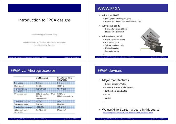
SLIDE 6

Joachim Rodrigues, EIT, LTH, Introduction to Structured VLSI Design jrs@eit.lth.se FPGA Intro

Delay‐Locked Loop (DLL)

  • Consists of a variable delay line and

control logic. Produces a delayed version of the input clock

  • Clock distribution network routes

the clock to all internal registers and feedback CLKFB pin.

  • Control logic samples the input clock

as well as the feedback clock in

  • rder to adjust the delay line.
  • Delay line is built as a series of

discrete delay elements.

  • A DLL inserts a delay between the

input clock and the feedback clock until the two rising edges align.

  • After the edges from the input clock

line up with the edges from the feedback clock, the DLL "locks."

Joachim Rodrigues, EIT, LTH, Introduction to Structured VLSI Design jrs@eit.lth.se FPGA Intro

DCM‐ Module Block Diagram

Remember: DCM is optional. If only one clock is required the

  • rdinary clock network can be used.

Joachim Rodrigues, EIT, LTH, Introduction to Structured VLSI Design jrs@eit.lth.se FPGA Intro

DCM‐ VHDL

DCM_inst : DCM generic map ( CLKDV_DIVIDE => 2.0, ‐‐ Divide by CLKFX_DIVIDE => 1, ‐‐ integer from 1 to 32 CLKFX_MULTIPLY => 4, ‐‐ integer from 1 to 32 CLKIN_DIVIDE_BY_2 => FALSE, ‐‐ TRUE/FALSE CLKIN_PERIOD => 0.0, ‐‐ period of input clock CLKOUT_PHASE_SHIFT => "NONE", ‐‐ CLK_FEEDBACK => "1X", ‐‐ feedback NONE, 1X or 2 DESKEW_ADJUST => "SYSTEM_SYNCHRONOUS", ‐‐ DFS_FREQUENCY_MODE => "LOW", ‐ DLL_FREQUENCY_MODE => "LOW", ‐ DUTY_CYCLE_CORRECTION => TRUE, ‐‐ Duty cycle FACTORY_JF => X"C080", ‐‐ FACTORY JF Values PHASE_SHIFT => 0, ‐‐ Amount of fixed phase shift SIM_MODE => "SAFE", DCM_inst : DCM generic map ( CLKDV_DIVIDE => 2.0, ‐‐ Divide by CLKFX_DIVIDE => 1, ‐‐ integer from 1 to 32 CLKFX_MULTIPLY => 4, ‐‐ integer from 1 to 32 CLKIN_DIVIDE_BY_2 => FALSE, ‐‐ TRUE/FALSE CLKIN_PERIOD => 0.0, ‐‐ period of input clock CLKOUT_PHASE_SHIFT => "NONE", ‐‐ CLK_FEEDBACK => "1X", ‐‐ feedback NONE, 1X or 2 DESKEW_ADJUST => "SYSTEM_SYNCHRONOUS", ‐‐ DFS_FREQUENCY_MODE => "LOW", ‐ DLL_FREQUENCY_MODE => "LOW", ‐ DUTY_CYCLE_CORRECTION => TRUE, ‐‐ Duty cycle FACTORY_JF => X"C080", ‐‐ FACTORY JF Values PHASE_SHIFT => 0, ‐‐ Amount of fixed phase shift SIM_MODE => "SAFE", STARTUP_WAIT => FALSE) ‐‐ port map ( CLK0 => CLK0, ‐‐ 0 degree DCM CLK ouptput CLK180 => CLK180, ‐‐ 180 degree DCM CLK output CLK270 => CLK270, ‐‐ 270 degree DCM CLK output CLK2X => CLK2X, ‐‐ 2X DCM CLK output CLK2X180 => CLK2X180, ‐‐ 2X, 180 CLK90 => CLK90, ‐‐ 90 degree DCM CLK output CLKDV => CLKDV, ‐‐ (CLKDV_DIVIDE) CLKFX => CLKFX, ‐‐ DCM CLK synthesis out (M/D) CLKFX180 => CLKFX180, ‐‐ LOCKED => LOCKED, ‐‐ DCM LOCK status output PSDONE => PSDONE, ‐‐ STATUS => STATUS, ‐‐ 8‐bit DCM status bits CLKFB => CLKFB, ‐‐ DCM clock feedback CLKIN => CLKIN, ‐‐ Clock input (IBUFG, BUFG,DCM) PSCLK => PSCLK, ‐‐ PSEN => PSEN, ‐‐ Dynamic phase adjust enable PSINCDEC => PSINCDEC, ‐‐ Dynamic phase adjust RST => RST ‐‐ DCM asynchronous reset input ); ‐‐ End of DCM_inst instantiation STARTUP_WAIT => FALSE) ‐‐ port map ( CLK0 => CLK0, ‐‐ 0 degree DCM CLK ouptput CLK180 => CLK180, ‐‐ 180 degree DCM CLK output CLK270 => CLK270, ‐‐ 270 degree DCM CLK output CLK2X => CLK2X, ‐‐ 2X DCM CLK output CLK2X180 => CLK2X180, ‐‐ 2X, 180 CLK90 => CLK90, ‐‐ 90 degree DCM CLK output CLKDV => CLKDV, ‐‐ (CLKDV_DIVIDE) CLKFX => CLKFX, ‐‐ DCM CLK synthesis out (M/D) CLKFX180 => CLKFX180, ‐‐ LOCKED => LOCKED, ‐‐ DCM LOCK status output PSDONE => PSDONE, ‐‐ STATUS => STATUS, ‐‐ 8‐bit DCM status bits CLKFB => CLKFB, ‐‐ DCM clock feedback CLKIN => CLKIN, ‐‐ Clock input (IBUFG, BUFG,DCM) PSCLK => PSCLK, ‐‐ PSEN => PSEN, ‐‐ Dynamic phase adjust enable PSINCDEC => PSINCDEC, ‐‐ Dynamic phase adjust RST => RST ‐‐ DCM asynchronous reset input ); ‐‐ End of DCM_inst instantiation

Joachim Rodrigues, EIT, LTH, Introduction to Structured VLSI Design jrs@eit.lth.se FPGA Intro

ISE‐Coregen

  • The DCM can be

initialized by using coregen in ISE

slide-7
SLIDE 7

Joachim Rodrigues, EIT, LTH, Introduction to Structured VLSI Design jrs@eit.lth.se FPGA Intro

Clocking: problems / challenges

  • Clock skew and clock distribution

– becoming increasingly difficult to handle

  • The clock wastes power

– it causes considerable unnecessary activity

  • The clock forces all parts of the system to operate at

the same speed

– parts have different natural speeds

Joachim Rodrigues, EIT, LTH, Introduction to Structured VLSI Design jrs@eit.lth.se FPGA Intro

FPGA Design flow (I)

  • Synthesis

– Parses HDL design – Infers Xilinx primitives – Generates design netlist

  • Translate

– Merges incoming netlists and constraints into a design file

  • Map

– Maps (places) design into the available resources on the target device

  • Place and Route

– Places and routes design to the timing constraints

Joachim Rodrigues, EIT, LTH, Introduction to Structured VLSI Design jrs@eit.lth.se FPGA Intro

Synthesis Optimizations (I)

  • global_opt on|off

Optimization routines that operate on the fully assembled netlist after initial packing. These optimizations include logic remapping and trimming, logic and register replication. This option can optimize black‐ boxed portions of the design.

  • logic_opt on|off

Post‐placement logic restructuring. Operates on a placed netlist to

  • ptimize timing critical connections through restructuring and re‐

synthesis, followed by incremental placement and incremental timing

  • analysis. Option is enabled in conjunction with “‐timing”.

Joachim Rodrigues, EIT, LTH, Introduction to Structured VLSI Design jrs@eit.lth.se FPGA Intro

Synthesis Constraints

Area tp small large slow fast

fmax=1/tpmax

slide-8
SLIDE 8

Joachim Rodrigues, EIT, LTH, Introduction to Structured VLSI Design jrs@eit.lth.se FPGA Intro

Synthesis Constraints (II)

  • Under‐constraining in synthesis prevents it from generating the best
  • ptimizations → tightly constrain synthesis until the tool reports negative

slack.

  • Design reuse netlist used as “black‐boxes” in synthesis may limit the

amount of possible optimization. Synthesis has the capability in the traditional flow to “read” netlists from black‐boxes. This helps the tools analyze paths going to and coming from the black boxes. → add these black boxes to the synthesis project and this is where physical synthesis

  • ptions can have a great impact (optimization over design boundaries)

Joachim Rodrigues, EIT, LTH, Introduction to Structured VLSI Design jrs@eit.lth.se FPGA Intro

Constraints

Placement constraint

Constraint Reality

Joachim Rodrigues, EIT, LTH, Introduction to Structured VLSI Design jrs@eit.lth.se FPGA Intro