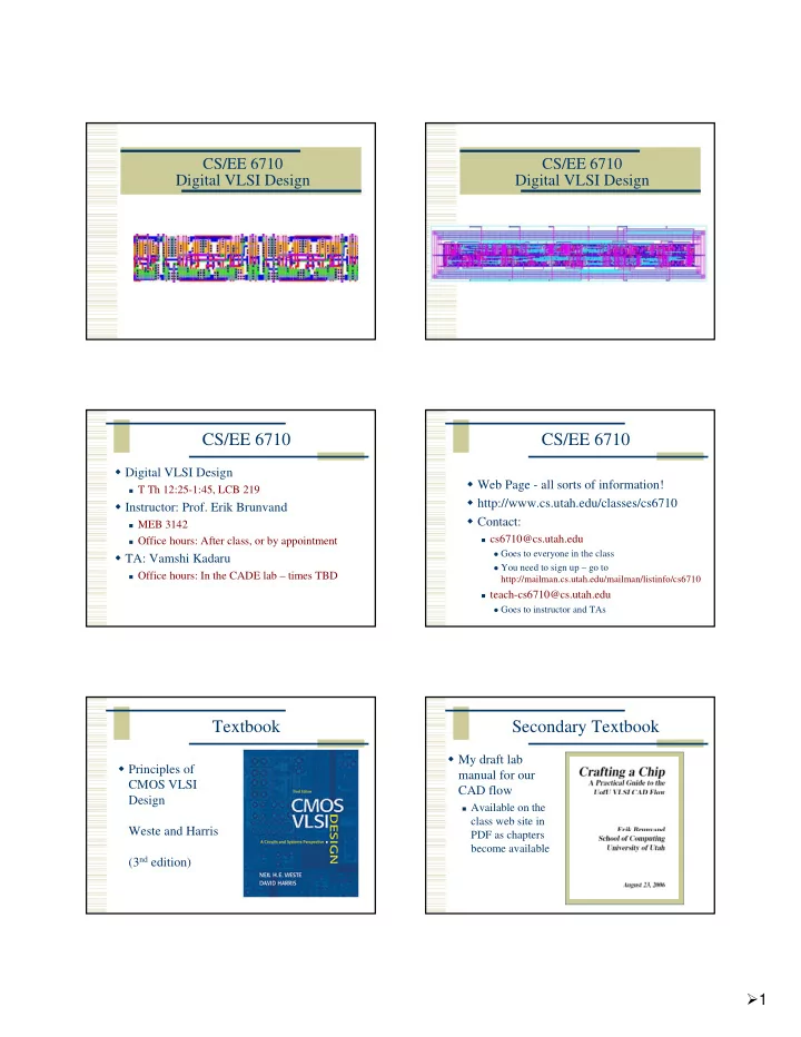
CS/EE 6710 CS/EE 6710 Digital VLSI Design Web Page - all sorts of - - PDF document

cs ee 6710 cs ee 6710
SMART_READER_LITE
LIVE PREVIEW

CS/EE 6710 CS/EE 6710 Digital VLSI Design Web Page - all sorts of - - PDF document

CS/EE 6710 CS/EE 6710 Digital VLSI Design Digital VLSI Design CS/EE 6710 CS/EE 6710 Digital VLSI Design Web Page - all sorts of information! T Th 12:25-1:45, LCB 219 http://www.cs.utah.edu/classes/cs6710 Instructor: Prof.


slide-1
SLIDE 1

1 CS/EE 6710 Digital VLSI Design CS/EE 6710 Digital VLSI Design

CS/EE 6710

Digital VLSI Design

T Th 12:25-1:45, LCB 219

Instructor: Prof. Erik Brunvand

MEB 3142 Office hours: After class, or by appointment

TA: Vamshi Kadaru

Office hours: In the CADE lab – times TBD

CS/EE 6710

Web Page - all sorts of information! http://www.cs.utah.edu/classes/cs6710 Contact:

cs6710@cs.utah.edu Goes to everyone in the class You need to sign up – go to

http://mailman.cs.utah.edu/mailman/listinfo/cs6710

teach-cs6710@cs.utah.edu Goes to instructor and TAs

Textbook

Principles of CMOS VLSI Design Weste and Harris (3nd edition)

Secondary Textbook

My draft lab manual for our CAD flow

Available on the

class web site in PDF as chapters become available

slide-2
SLIDE 2

2

Class Goal

To learn about modern digital CMOS IC design

Class project –

teams will build moderate sized chip

We’ll form teams in a few weeks Modulo funding constraints, these chips can be

fabricated through MOSIS

Chip fabrication service for small-volume projects Educational program funded entirely by MOSIS

Class Goal

We’ll use tools from Cadence and Synopsys

These only run on Solaris and Linux in the CADE

lab, so you’ll need a CADE account

I also assume you know something about UNIX

http://www.cs.utah.edu/classes/cs1010/

Prerequisites

Digital design is required! (i.e. CS/EE 3700)

Boolean algebra Combinational circuit design and optimization K-map minimization, SOP, POS, DeMorgan,

bubble-pushing, etc.

Arithmetic circuits, 2’s complement numbers Sequential Circuit design and optimization Latch/flip-flop design Finite state machine design/implementation Communicating FSMs Using FSMs to control datapaths

Assignment #1 – Review

On the class web site is a review assignment

If you can do these problems, you probably have

the right background

If you can’t, you will struggle!!!!!

Please take this seriously! Give this exam a try and make sure you remember what you need to know!

You also need to turn it in next week by

Friday September 1st

Grading is pass/fail

Recommendations

Computer Architecture experience is helpful

Instruction set architecture (ISA) Assembly language execution model Instruction encoding Simple pipelining

I assume you’ve used some sort of CAD tools for digital circuits

Schematic capture Simulation

First Assignment

CAD Assignment #1

Cadence Composer tutorial Simple circuit design with simulation Learn basic Verilog for testbench Available on the web site Due on Friday, September 1st, 5:00pm

slide-3
SLIDE 3

3

Assignments/Grading

Labs (cell designs) & Homework (40%) Design review (5%) Mid-term exam (15%) Final Project (40%)

See the syllabus (web page) for more details

about grading breakdown

The Big Picture

Physics Electronics VLSI Logic Gates FSM RTL

FSM

Computer

M OV R1 R2 ADD R1 R3 R5 ST R3 (5)R6

I SA

if (c==1) x = foo(y); else x = bar(a,b);

Progamming Languages

OS Compilers Algorithms Applications Etc...

Lightening Tour of VLSI Design

Start with HDL program (VHDL, Verilog)

entity traffic is port (CLK, go_green, go_red, go_yellow: in STD_LOGIC; l_green, l_red, l_yellow: out STD_LOGIC;); end; architecture traffic_arch of traffic is

  • - SYMBOLIC ENCODED state machine: Sreg0

type Sreg0_type is (green, red, yellow); signal Sreg0: Sreg0_type; begin

  • -concurrent signal assignments

Sreg0_machine: process (CLK) begin if CLK'event and CLK = '1' then case Sreg0 is when green => if go_yellow='1' then Sreg0 <= yellow; end if; when red => if go_green='1' then Sreg0 <= green; end if; when yellow => if go_red='1' then Sreg0 <= red; end if;

  • - when others =>

null; end case; end if; end process; assignment statements for combinatorial outputs l_green_assignment: l_green <= '1' when (Sreg0 = green) else '0' when (Sreg0 = red) else '0' when (Sreg0 = yellow) else '0'; l_yellow_assignment: l_yellow <= '0' when (Sreg0 = green) else '0' when (Sreg0 = red) else '1' when (Sreg0 = yellow) else '1'; l_red_assignment: l_red <= '0' when (Sreg0 = green) else '1' when (Sreg0 = red) else '0' when (Sreg0 = yellow) else '0'; end traffic_arch;

VLSI Design

Or start with a schematic (or a mix of both)

Convert Gates to Transistors Convert Transistors to Layout

slide-4
SLIDE 4

4

Assemble Gates into a Circuit And Assemble Whole Chip Example Class Chip (2001)

16-bit Processor, approx 27,000 transistors

Same Chip (no M2, M3)

1.5mm x 3.0mm, 72 I/O pads

Zoom In… Zoom In…

A Hair (100 microns)

slide-5
SLIDE 5

5

Another Class Project (2001)

3.0mm x 3.0mm 84 I/O Pads

Standard-Cell Part Standard-Cell Zoom Register File Adder/Shifter Class project from 2002

16-bit CORDIC Processor

slide-6
SLIDE 6

6

Class project from 2003

Basketball Scoreboard Display

Class project from 2003

Basketball Scoreboard Display

Another class project (2003)

Simple processor (+, -, *, /) with ADC on the input

Class project from 2005

Bomb game With VGA

  • utput

Bomb game from 2005 Bomb game from 2005

slide-7
SLIDE 7

7

Fabricate and Test the Chip

We can fabricate the chips through MOSIS

Educational program sponsored by MOSIS’ commercial

activities

Chips are fabricated, packaged, and shipped back to us

Then we get to test them to see what they do, or don’t do… Not necessarily a research area in its own right here at Utah

But, a powerful tool for hardware-related research

projects!

IC Technology

We’ll use the AMI 0.6u 3-level-metal CMOS process

We have technology files that define the process MOSIS Scalable CMOS Rev. 8 (SCMOS) Tech files from NCSU CDK NCSU toolkit is designed for custom VLSI layout Design Rule Check (DRC) rules Layout vs. Schematic (LVS) rules

Class Project

Standard Cell Library

Each group will design a small, but useful,

standard cell library

Use HDL synthesis with this library as a target Use Cadence SOC Encounter for place and route

Custom Datapath

Use ICC router to connect HDL-Synthesized

control to custom-designed datapath

It will be VERY helpful to have a mix of

knowledge on your team

Class Project

Two complete design views: Schematic and Layout

Complete design in Composer schematics,

simulated with Verilog

Complete design at layout level in Virtuoso with

detailed simulation using Spectre

Validate they are the same with LVS

Custom layout for datapath Synthesized controller using Synopsys, SOC Encounter, and your cell library Final assembly back in Virtuoso

Timetable

This project will be a race to the finish!

There is no slack in this schedule!!!

VLSI design always takes longer than you think

Even if you take that rule into account!

After you have 90% finished, there’s only 90% left…

All team members will have to contribute! Team peer evaluations twice a semester

A View of the Tools

Synopsys Synthesis

Cadence SOC Encounter Cadence Composer Schematic Cadence Virtuoso Layout AutoRouter (SOC or ccar) Your Library Verilog-XL Verilog-XL Behavioral Verilog Structural Verilog Circuit Layout LVS

Layout-XL

CSI Spectre

slide-8
SLIDE 8

8

A View of the Tools

Synopsys Synthesis

Cadence SOC Encounter Cadence Composer Schematic Cadence Virtuoso Layout AutoRouter (SOC or ccar) Your Library Verilog-XL Verilog-XL Behavioral Verilog Structural Verilog Circuit Layout LVS

Layout-XL

CSI Spectre CAD1

A View of the Tools

Synopsys Synthesis

Cadence SOC Encounter Cadence Composer Schematic Cadence Virtuoso Layout AutoRouter (SOC or ccar) Your Library Verilog-XL Verilog-XL Behavioral Verilog Structural Verilog Circuit Layout LVS

Layout-XL

CSI Spectre CAD2

Cadence Composer Schematic Cadence Composer Schematic Cadence Composer Symbol Cadence Virtuoso Layout

slide-9
SLIDE 9

9

Standard Cells…Power Rings Place Cells and Fillers Connect Rows to Power autoRouted View autoRouted Layout View Corners…

slide-10
SLIDE 10

10

Routing Slightly Larger Example Electronics Summary

Voltage is a measure of electrical potential energy Current is moving charge caused by voltage Resistance reduces current flow

Ohm’s Law: V = I R

Power is work over time

P = V I = I2R = V2/R

Capacitors store charge

It takes time to charge/ discharge a capacitor Time to charge/discharge is related exponentially to RC It takes energy to charge a capacitor Energy stored in a capacitor is (1/2)CV2

Energy (joules): work required to move one coulomb of charge by one volt or work done to produce one watt for one sec

Reminder: Voltage Division

Find the voltage across any series-connected resistors

Example of Voltage Division

Find the voltage at point A with respect to GND

Example of Voltage Division

Find the voltage at point A with respect to GND

slide-11
SLIDE 11

11

How Does This Relate to VLSI? Model of a CMOS Transistor Two Types of CMOS Transistors CMOS Transistors

Complementary Metal Oxide Semiconductor Two types of transistors

Built on silicon substrate “majority carrier” devices Field-effect transistors An electric field attracts carriers to form a conducting

channel in the silicon…

We’ll get much more of this later… For now, just some basic abstractions

Silicon Lattice

Transistors are built on a silicon substrate Silicon is a Group IV material Forms crystal lattice with bonds to four neighbors

Figures from Reid Harrison

“Semi” conductor?

Thermal energy (atomic-scale vibrations) can shake an electron loose

Leaves a “hole” behind Figures from Reid Harrison

slide-12
SLIDE 12

12

“Semi” conductor?

Room temperature: 1.5x10¹⁰ free electrons per cubic

centimeter

But, 5x10²² silicon atoms / cc So, one out of every 3 trillion atoms has a missing e

Figures from Reid Harrison

Dopants

Group V: extra electron (n-type)

Phosphorous, Arsenic,

Group III: missing electron, (p-type)

Usually Boron Figures from Reid Harrison

Dopants

Note that each type of doped silicon is electrostatically neutral in the large

Consists of mobile electrons and holes And fixed charges (dopant atoms) Figures from Reid Harrison

p-n Junctions

A junction between p-type and n-type semiconductor forms a diode. Current flows only in one direction p-type n-type anode cathode

p-n Junctions

Two mechanisms for carrier (hole or electron)

motion

Drift - requires an electric field Diffusion – requires a concentration gradient

Figures from Reid Harrison

p-n Junctions

With no external voltage diffusion causes a

depletion region

Causes an

electric field because of charge recombination

Causes drift

current…

Figures from Reid Harrison

slide-13
SLIDE 13

13

p-n Junctions

Eventually reaches equilibrium where diffusion

current offsets drift current

Figures from Reid Harrison

p-n Junctions

By applying an external voltage you can modulate

the width fo the depletion region and cause diffusion

  • r drift to dominate…

Figures from Reid Harrison

+

  • i

electrons Vds +Vgs S G D

N-type Transistor nMOS Operation

Body is commonly tied to ground (0 V) When the gate is at a low voltage:

P-type body is at low voltage Source-body and drain-body diodes are OFF No current flows, transistor is OFF n+ p Gate Source Drain bulk Si SiO2 Polysilicon n+ D S

nMOS Operation Cont.

When the gate is at a high voltage:

Positive charge on gate of MOS capacitor Negative charge attracted to body Inverts a channel under gate to n-type Now current can flow through n-type silicon

from source through channel to drain, transistor is ON

n+ p Gate Source Drain bulk Si SiO2 Polysilicon n+ D 1 S

+

  • i

holes Vsd

  • Vgs

S G D

P-type Transistor

slide-14
SLIDE 14

14

pMOS Transistor

Similar, but doping and voltages reversed

Body tied to high voltage (VDD) Gate low: transistor ON Gate high: transistor OFF Bubble indicates inverted behavior SiO2 n Gate Source Drain bulk Si Polysilicon p+ p+

A Cutaway View

CMOS structure with both transistor types

Transistors as Switches

For now, we’ll abstract away most analog details…

S G D S G D G=0 G=1 G=0 G=1 Good 0 Poor 0 Good 1 Poor 1 Good 1 Good 0 Good 1 Good 0 Not Perfect Switches!

“Switching Circuit”

For example, a switch can control when a light comes on or off

No electricity can flow +5v 0v

“AND” Circuit

Both switch X AND switch Y need to be closed for the light to light up

+5v 0v

X Y

“OR” Circuit

The light comes on if either X OR Y are closed

+5v

X Y

0v

slide-15
SLIDE 15

15

CMOS Inverter CMOS Inverter

1 Y A

VDD A Y GND

A Y

CMOS Inverter

1 Y A

VDD

A=1 Y=0

GND ON OFF

A Y

CMOS Inverter

1 1 Y A

VDD

A=0 Y=1

GND OFF ON

A Y

Timing Issues in CMOS Power Consumption

slide-16
SLIDE 16

16

CMOS NAND Gate CMOS NAND Gate

1 1 A 1 1 Y B

A B Y CMOS NAND Gate

1 1 A 1 1 1 Y B A=0 B=0 Y=1 OFF ON ON OFF

CMOS NAND Gate

1 1 A 1 1 1 1 Y B A=0 B=1 Y=1 OFF OFF ON ON

CMOS NAND Gate

1 1 A 1 1 1 1 1 Y B A=1 B=0 Y=1 ON ON OFF OFF

CMOS NAND Gate

1 1 A 1 1 1 1 1 Y B A=1 B=1 Y=0 ON OFF OFF ON

slide-17
SLIDE 17

17

CMOS NOR Gate 3-input NAND Gate

Y pulls low if ALL inputs are 1 Y pulls high if ANY input is 0

3-input NAND Gate

Y pulls low if ALL inputs are 1 Y pulls high if ANY input is 0 A B Y C

N-type and P-type Uses

Because of the imperfect nature of the the transistor switches

ALWAYS use N-type to pull low ALWAYS use P-type to pull high If you need to pull both ways, use them both

S In Out S S=0, In = Out S=1, In = Out

Switch to Chalkboard

Complex Gate Tri-State Latch D-register XOR