electronics summary
play

Electronics Summary CS/ECE 5710/6710 Digital VLSI Design Voltage - PDF document

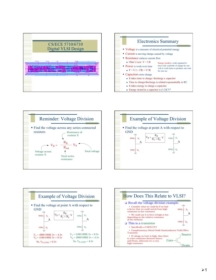
Electronics Summary CS/ECE 5710/6710 Digital VLSI Design Voltage is a measure of electrical potential energy Current is moving charge caused by voltage Resistance reduces current flow Ohms Law: V = I R Energy (joules): work


  1. Electronics Summary CS/ECE 5710/6710 Digital VLSI Design  Voltage is a measure of electrical potential energy  Current is moving charge caused by voltage  Resistance reduces current flow  Ohm’s Law: V = I R Energy (joules): work required to  Power is work over time move one coulomb of charge by one volt or work done to produce one watt  P = V I = I 2 R = V 2 /R for one sec  Capacitors store charge  It takes time to charge/ discharge a capacitor  Time to charge/discharge is related exponentially to RC  It takes energy to charge a capacitor  Energy stored in a capacitor is (1/2)CV 2 Reminder: Voltage Division Example of Voltage Division  Find the voltage across any series-connected  Find the voltage at point A with respect to resistors GND How Does This Relate to VLSI? Example of Voltage Division  Find the voltage at point A with respect to GND  1

  2. Two Types of CMOS Transistors Model of a CMOS Transistor CMOS Transistors Silicon Lattice  Transistors are built on a silicon substrate  Complementary Metal Oxide Semiconductor  Silicon is a Group IV material  Two types of transistors  Forms crystal lattice with bonds to four  Built on silicon substrate neighbors  “majority carrier” devices  Field-effect transistors  An electric field attracts carriers to form a conducting channel in the silicon…  We’ll get much more of this later…  For now, just some basic abstractions Figures from Reid Harrison “Semi” conductor? “Semi” conductor?  Thermal energy (atomic-scale vibrations) can  Room temperature: 1.5x10 10 free electrons per cubic centimeter shake an electron loose  But, 5x10 22 silicon atoms / cc  Leaves a “hole” behind  So, one out of every 3 trillion atoms has a missing e Figures from Reid Harrison Figures from Reid Harrison  2

  3. Dopants Dopants  Group V: extra electron (n-type)  Note that each type of doped silicon is electrostatically neutral in the large  Phosphorous, Arsenic,  Consists of mobile electrons and holes  Group III: missing electron, (p-type)  And fixed charges (dopant atoms)  Usually Boron Figures from Reid Harrison Figures from Reid Harrison p-n Junctions p-n Junctions  A junction between p-type and n-type  Two mechanisms for carrier (hole or electron) motion semiconductor forms a diode.  Drift - requires an electric field  Current flows only in one direction  Diffusion – requires a concentration gradient Figures from Reid Harrison p-n Junctions p-n Junctions  With no external voltage diffusion causes a  Eventually reaches equilibrium where diffusion depletion region current offsets drift current  Causes an electric field because of charge recombination  Causes drift current… Figures from Reid Harrison Figures from Reid Harrison  3

  4. N-type Transistor p-n Junctions  By applying an external voltage you can modulate the width of the depletion region and cause diffusion or drift to dominate… D + G Vds i electrons S - +Vgs Figures from Reid Harrison nMOS Operation nMOS Operation Cont.  Body is commonly tied to ground (0 V)  When the gate is at a high voltage:  When the gate is at a low voltage:  Positive charge on gate of MOS capacitor  Negative charge attracted to body  P-type body is at low voltage  Inverts a channel under gate to n-type  Source-body and drain-body diodes are OFF  Now current can flow through n-type silicon  No current flows, transistor is OFF from source through channel to drain, transistor is ON P-type Transistor pMOS Transistor  Similar, but doping and voltages reversed  Body tied to high voltage (V DD )  Gate low: transistor ON  Gate high: transistor OFF  Bubble indicates inverted behavior S + -Vgs G Vsd i holes - D  4

  5. A Cutaway View Transistors as Switches  CMOS structure with both transistor types  For now, we’ll abstract away most analog details… D Good 0 Good 1 G G=0 G=1 S Poor 1 Good 0 S Good 0 Good 1 G G=0 G=1 D Poor 0 Good 1 Not Perfect Switches! “Switching Circuit” “AND” Circuit  For example, a switch can control when a  Both switch X AND switch Y need to be light comes on or off closed for the light to light up +5v +5v X No electricity can flow Y 0v 0v “OR” Circuit CMOS Inverter  The light comes on if either X OR Y are closed +5v X Y 0v  5

  6. CMOS Inverter CMOS Inverter A Y A Y 0 0 1 1 ? CMOS Inverter CMOS Inverter A Y A Y 0 0 1 1 0 1 0 Timing Issues in CMOS Power Consumption  6

  7. CMOS NAND Gate CMOS NAND Gate A B Y 0 0 0 1 1 0 1 1 CMOS NAND Gate CMOS NAND Gate A B Y A B Y 0 0 1 0 0 1 0 1 0 1 1 1 0 1 0 1 1 1 1 CMOS NAND Gate CMOS NAND Gate A B Y A B Y 0 0 1 0 0 1 0 1 1 0 1 1 1 0 1 1 0 1 1 1 1 1 0  7

  8. CMOS NOR Gate 3-input NAND Gate  Y pulls low if ALL inputs are 1  Y pulls high if ANY input is 0 3-input NAND Gate N-type and P-type Uses  Because of the imperfect nature of the the  Y pulls low if ALL inputs are 1 transistor switches  Y pulls high if ANY input is 0  ALWAYS use N-type to pull low  ALWAYS use P-type to pull high  If you need to pull both ways, use them both In S=0, In = Out S S S=1, In = Out Out Switch to Chalkboard  Complex Gate  Tri-State  Latch  D-register  XOR  8

Download Presentation
Download Policy: The content available on the website is offered to you 'AS IS' for your personal information and use only. It cannot be commercialized, licensed, or distributed on other websites without prior consent from the author. To download a presentation, simply click this link. If you encounter any difficulties during the download process, it's possible that the publisher has removed the file from their server.

Recommend


More recommend