
SLIDE 1
- 1
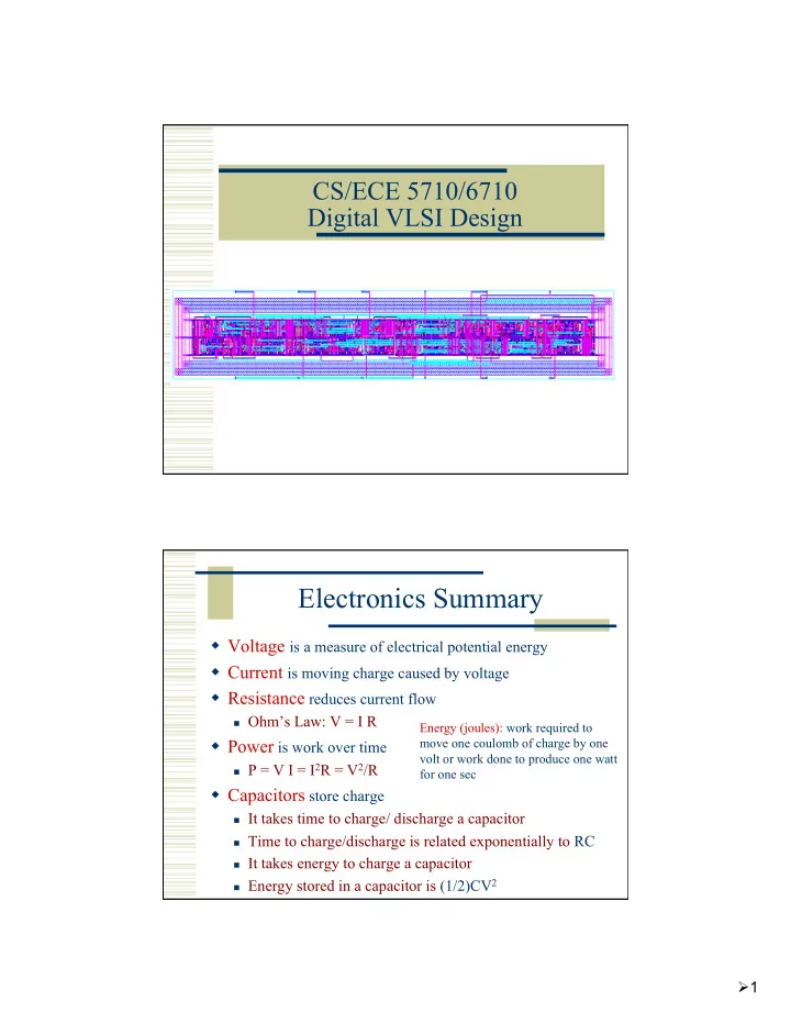
CS/ECE 5710/6710 Digital VLSI Design
Electronics Summary
Voltage is a measure of electrical potential energy Current is moving charge caused by voltage Resistance reduces current flow
Ohm’s Law: V = I R
Power is work over time
P = V I = I2R = V2/R
Capacitors store charge
It takes time to charge/ discharge a capacitor Time to charge/discharge is related exponentially to RC It takes energy to charge a capacitor Energy stored in a capacitor is (1/2)CV2
Energy (joules): work required to move one coulomb of charge by one volt or work done to produce one watt for one sec