
SLIDE 1
EEL7312 – INE5442 Digital Integrated Circuits 1
Capacitance - 1
Source: wikipedia
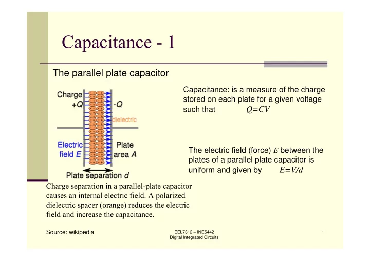
The parallel plate capacitor
Charge separation in a parallel-plate capacitor causes an internal electric field. A polarized dielectric spacer (orange) reduces the electric field and increase the capacitance. Capacitance: is a measure of the charge stored on each plate for a given voltage such that Q=CV The electric field (force) E between the plates of a parallel plate capacitor is uniform and given by E=V/d