
SLIDE 1
2-7.1
Spiral 2-7
Capacitance, Delay and Sizing
2-7.2
Learning Outcomes
- I understand the sources of capacitance in CMOS circuits
- I understand how delay scales with resistance, capacitance
and voltage
- I can determine appropriate width of PMOS and NMOS
transistors based on the configuration of the transistors and given current conduction parameters
- I understand how fan-in and fan-out affect the delay of a
circuit
– I understand how to use sizing to drive larger fan-out loads
- I understand the sources of static and dynamic power
consumption and how they are affect by changes in various parameters
2-7.3
WHAT IS CAPACITANCE?
2-7.4
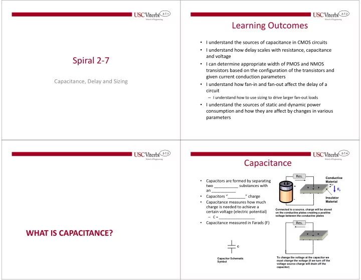
Capacitance
- Capacitors are formed by separating
two ___________ substances with an ___________
- Capacitors “________” charge
- Capacitance measures how much
charge is needed to achieve a certain voltage (electric potential)
– C = __________________
- Capacitance measured in Farads (F)
Conductive Material Insulator Material +
- +
+ +
- Connected to a source, charge will be stored
- n the conductive plates creating a positive
voltage between the conductive plates To change the voltage at the capacitor we must change the voltage (if we turn off the voltage source charge will drain off the capacitor) Capacitor Schematic Symbol C
+ + +
- Ey
Res. Res.