Transistors ENGR 40M lecture notes July 10, 2017 Chuan-Zheng Lee, - - PDF document

transistors
SMART_READER_LITE
LIVE PREVIEW

Transistors ENGR 40M lecture notes July 10, 2017 Chuan-Zheng Lee, - - PDF document

Transistors ENGR 40M lecture notes July 10, 2017 Chuan-Zheng Lee, Stanford University A transistor is an electronic device that is used to allow one electrical signal to control another electrical signal, typically larger in either voltage or


slide-1
SLIDE 1

Transistors

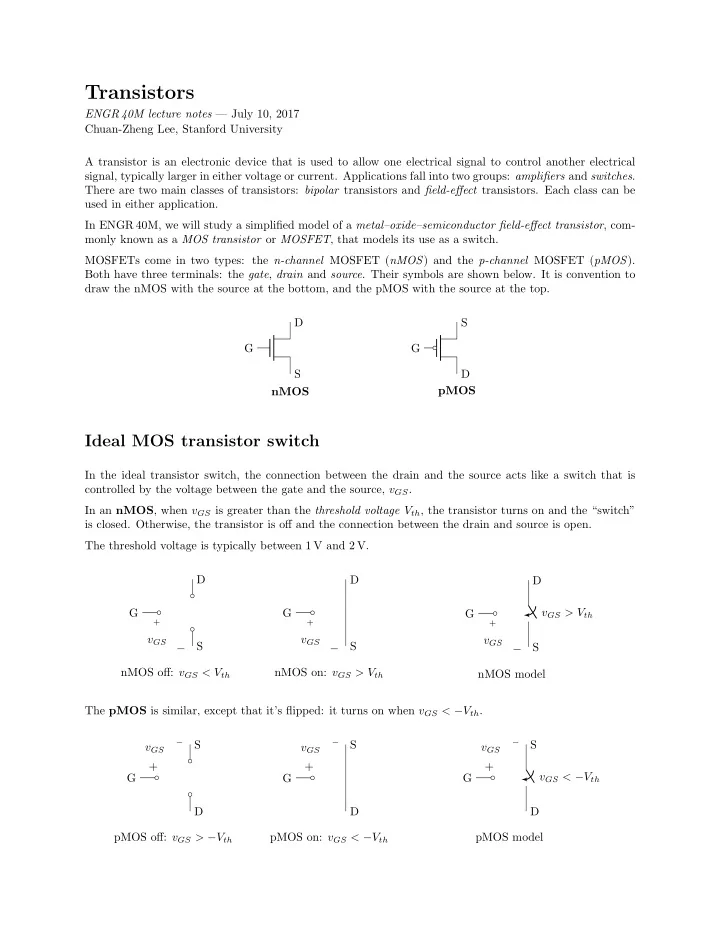
ENGR 40M lecture notes — July 10, 2017 Chuan-Zheng Lee, Stanford University A transistor is an electronic device that is used to allow one electrical signal to control another electrical signal, typically larger in either voltage or current. Applications fall into two groups: amplifiers and switches. There are two main classes of transistors: bipolar transistors and field-effect transistors. Each class can be used in either application. In ENGR 40M, we will study a simplified model of a metal–oxide–semiconductor field-effect transistor, com- monly known as a MOS transistor or MOSFET, that models its use as a switch. MOSFETs come in two types: the n-channel MOSFET (nMOS) and the p-channel MOSFET (pMOS). Both have three terminals: the gate, drain and source. Their symbols are shown below. It is convention to draw the nMOS with the source at the bottom, and the pMOS with the source at the top. G D S nMOS G D S pMOS

Ideal MOS transistor switch

In the ideal transistor switch, the connection between the drain and the source acts like a switch that is controlled by the voltage between the gate and the source, vGS. In an nMOS, when vGS is greater than the threshold voltage Vth, the transistor turns on and the “switch” is closed. Otherwise, the transistor is off and the connection between the drain and source is open. The threshold voltage is typically between 1 V and 2 V. G D S

+

− vGS nMOS off: vGS < Vth G D S

+

− vGS nMOS on: vGS > Vth G D vGS > Vth S

+

− vGS nMOS model The pMOS is similar, except that it’s flipped: it turns on when vGS < −Vth. G S D

+ vGS pMOS off: vGS > −Vth G S D

+ vGS pMOS on: vGS < −Vth G S vGS < −Vth D

+ vGS pMOS model

slide-2
SLIDE 2

Modeling internal resistance

Real transistors aren’t perfect open circuits when off and perfect short circuits when on. In practice, there is a large resistance when off, and a small resistance when on. In some applications, this resistance can be signficant, and needs to be accounted for when designing your circuit. We call the “off resistance” Roff, and the “on resistance” Ron. G D Roff S

+

− vGS nMOS off: vGS < Vth G D Ron S

+

− vGS nMOS on: vGS > Vth G S Roff D

+ vGS pMOS off: vGS > −Vth G S Ron D

+ vGS pMOS on: vGS < −Vth

Usage notes

  • Because the source is involved in both the “input” (gate) and “output” (drain), it is common to connect

the source to a known, stable reference point.

  • Because, for an nMOS, vGS has to be (very) positive to turn the transistor on, it is common for this

reference point to be ground. Similarly, for a pMOS, since vGS has to be (very) negative to turn the transistor on, it is common for this reference point to be VDD. Special penalties will apply if you connect the source of an nMOS to VDD, or the source of a pMOS to ground, in a circuit that you draw in homework, prelabs, labs or an exam.

  • In many (digital) circuits, including most (but not all!) circuits that we will study in this class, the

input voltage is by design always VDD or 0 V, i.e. always well below or well above the threshold voltage.

  • Note that, in our model, there is never any current going into the gate of a MOS transistor.

2

slide-3
SLIDE 3

Examples

Unless otherwise specified, VDD = 5 V, and Vth = 1 V for all transistors. Example 1. In the circuit below, (a) what is vout? (b) what is iD? VDD 1 kΩ iD VDD vout Example 2. In the circuit below, (a) what is vout? (b) what is iD? 1 kΩ iD VDD vout The next example shows that putting a load on the output changes the behavior of the circuit in Example 2. Example 3. In the circuit below, what is the current through the LED? 1 kΩ iD VDD Vf = 2 V 300 Ω It might be tempting to resolve the problem in Example 3 by connecting the nMOS to VDD instead. Unfor- tunately, this doesn’t work. 3

slide-4
SLIDE 4

Example 4. In the circuit below, if Vth = 2 V, what values of vin would turn the transistor on? − + vin S VDD D 1 kΩ vout This illuminates one problem: we need voltages higher than VDD, which you don’t have access to in most

  • circuits. In fact, this isn’t the only problem. In many transistors, when placed in this configuration, the

drain will behave like a source and vice versa, and the transistor will no longer act as a switch, making our model inappropriate. For digital circuits, an nMOS can’t be used like this: a pMOS must be used to make connections to VDD. Example 5. What is vout when (a) vin = VDD, (b) vin = 0 V? − + vin VDD 1 kΩ vout Example 6. Repeat Example 5 with Roff = 100 kΩ and Ron = 50 Ω. Example 7. For both transistors, Roff = 100 kΩ and Ron = 50 Ω. Find vout when (a) vin = VDD, (b) vin = 0 V. VDD vin vout 4