
SLIDE 1
Bipolar Junction Transistors
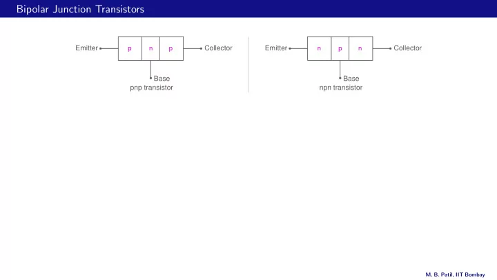
Base Emitter Collector Base Emitter Collector npn transistor pnp transistor
p n p n p n
- M. B. Patil, IIT Bombay
Bipolar Junction Transistors Emitter p n p Collector Emitter n - - PowerPoint PPT Presentation
Bipolar Junction Transistors Emitter p n p Collector Emitter n p n Collector Base Base pnp transistor npn transistor M. B. Patil, IIT Bombay Bipolar Junction Transistors Emitter p n p Collector Emitter n p n Collector Base
Base Emitter Collector Base Emitter Collector npn transistor pnp transistor
p n p n p n
Base Emitter Collector Base Emitter Collector npn transistor pnp transistor
p n p n p n
Base Emitter Collector Base Emitter Collector npn transistor pnp transistor
p n p n p n
Base Emitter Collector Base Emitter Collector npn transistor pnp transistor
p n p n p n
When Bell Labs had an informal contest to name their new invention, one engineer pointed out that it acts like a resistor, but a resistor where the voltage is transferred across the device to control the resulting current. (http://amasci.com/amateur/trshort.html)
p n p B C E 5 V 10 V
I3 I1 I2 1 k 1 k R1 R2
p n p B C E 5 V 10 V
I3 I1 I2 1 k 1 k R1 R2
D1 D2 B E C 5 V 10 V
I3 I2 I1 1 k 1 k R2 R1
p n p B C E 5 V 10 V
I3 I1 I2 1 k 1 k R1 R2
D1 D2 B E C 5 V 10 V
I3 I2 I1 1 k 1 k R2 R1
10 V 10 V B 5 V E C p n p B C E 5 V
R1 1 k I3 I2 I1 α I1 I3 I1 I2 1 k 1 k 1 k R2 R1 R2
10 V 10 V B 5 V E C p n p B C E 5 V
R1 1 k I3 I2 I1 α I1 I3 I1 I2 1 k 1 k 1 k R2 R1 R2
10 V 10 V B 5 V E C p n p B C E 5 V
R1 1 k I3 I2 I1 α I1 I3 I1 I2 1 k 1 k 1 k R2 R1 R2
10 V 10 V B 5 V E C p n p B C E 5 V
R1 1 k I3 I2 I1 α I1 I3 I1 I2 1 k 1 k 1 k R2 R1 R2
10 V 10 V B 5 V E C p n p B C E 5 V
R1 1 k I3 I2 I1 α I1 I3 I1 I2 1 k 1 k 1 k R2 R1 R2
10 V 10 V B 5 V E C p n p B C E 5 V
R1 1 k I3 I2 I1 α I1 I3 I1 I2 1 k 1 k 1 k R2 R1 R2
p D1 n p Base Emitter Base Collector Collector D2 Emitter
p D1 n p Base Emitter Base Collector Collector D2 Emitter
p n p Emitter Collector Base
p D1 n p Base Emitter Base Collector Collector D2 Emitter
p n p Emitter Collector Base
n p p n p n B E B C B E C B E C E C
IC IC IC IE IC IE IE IB IE IB IB IB
n p p n p n B E B C B E C B E C E C
IC IC IC IE IC IE IE IB IE IB IB IB
n p p n p n B E B C B E C B E C E C
IC IC IC IE IC IE IE IB IE IB IB IB
n p p n p n B E B C B E C B E C E C
IC IC IC IE IC IE IE IB IE IB IB IB
n p p n p n B E B C B E C B E C E C
IC IC IC IE IC IE IE IB IE IB IB IB
n p p n p n B E B C B E C B E C E C
IC IC IC IE IC IE IE IB IE IB IB IB
E B C E B C E C B E B C E B C n p p n p n B E C
IC IC IE IE IB IB α IE α IE IC IC IC IE IC IE IE IB IE IB IB IB
E B C E B C E C B E B C E B C n p p n p n B E C
IC IC IE IE IB IB α IE α IE IC IC IC IE IC IE IE IB IE IB IB IB
E B C E B C E C B E B C E B C n p p n p n B E C
IC IC IE IE IB IB α IE α IE IC IC IC IE IC IE IE IB IE IB IB IB
E B C E B C E C B E B C E B C n p p n p n B E C
IC IC IE IE IB IB α IE α IE IC IC IC IE IC IE IE IB IE IB IB IB
E B C E B C E C B E B C E B C n p p n p n B E C
IC IC IE IE IB IB α IE α IE IC IC IC IE IC IE IE IB IE IB IB IB
E B C E B C E C B E B C E B C n p p n p n B E C
IC IC IE IE IB IB α IE α IE IC IC IC IE IC IE IE IB IE IB IB IB
E B C E B C E C B E B C E B C n p p n p n B E C
IC IC IE IE IB IB α IE α IE IC IC IC IE IC IE IE IB IE IB IB IB
E B C E B C E C B E B C E B C n p p n p n B E C
IC IC IE IE IB IB α IE α IE IC IC IC IE IC IE IE IB IE IB IB IB
E B C E B C E C B E B C E B C n p p n p n B E C
IC IC IE IE IB IB α IE α IE IC IC IC IE IC IE IE IB IE IB IB IB
E B C E B C E C B E B C E B C n p p n p n B E C
IC IC IE IE IB IB α IE α IE IC IC IC IE IC IE IE IB IE IB IB IB
RB RC VCC VBB B C E 10 V 2 V 1 k 100 k β = 100
RB RC VCC VBB B C E 10 V 2 V 1 k 100 k β = 100
p n n
RB RC VCC VBB 10 V 2 V 1 k 100 k
RB RC VCC VBB B C E 10 V 2 V 1 k 100 k β = 100
p n n
RB RC VCC VBB 10 V 2 V 1 k 100 k IC IB IE αIE RB RC VCC VBB 10 V 2 V 1 k 100 k
RB RC VCC VBB B C E 10 V 2 V 1 k 100 k β = 100
p n n
RB RC VCC VBB 10 V 2 V 1 k 100 k IC IB IE αIE RB RC VCC VBB 10 V 2 V 1 k 100 k
RB RC VCC VBB B C E 10 V 2 V 1 k 100 k β = 100
p n n
RB RC VCC VBB 10 V 2 V 1 k 100 k IC IB IE αIE RB RC VCC VBB 10 V 2 V 1 k 100 k
RB RC VCC VBB B C E 10 V 2 V 1 k 100 k β = 100
p n n
RB RC VCC VBB 10 V 2 V 1 k 100 k IC IB IE αIE RB RC VCC VBB 10 V 2 V 1 k 100 k
RB RC VCC VBB B C E 10 V 2 V 1 k 100 k β = 100
p n n
RB RC VCC VBB 10 V 2 V 1 k 100 k IC IB IE αIE RB RC VCC VBB 10 V 2 V 1 k 100 k
RB RC VCC VBB B C E 10 V 2 V 1 k 100 k β = 100
p n n
RB RC VCC VBB 10 V 2 V 1 k 100 k IC IB IE αIE RB RC VCC VBB 10 V 2 V 1 k 100 k
RB RC VCC VBB B C E 10 V 2 V 1 k 100 k β = 100
p n n
RB RC VCC VBB 10 V 2 V 1 k 100 k IC IB IE αIE RB RC VCC VBB 10 V 2 V 1 k 100 k
p n n
IC IB IE αIE RB RB RB RC RC RC VCC VBB VCC VBB VCC VBB B C E 10 V 2 V 10 V 2 V 10 V 2 V 1 k 10 k 1 k 10 k 1 k 10 k β = 100
p n n
IC IB IE αIE RB RB RB RC RC RC VCC VBB VCC VBB VCC VBB B C E 10 V 2 V 10 V 2 V 10 V 2 V 1 k 10 k 1 k 10 k 1 k 10 k β = 100
p n n
IC IB IE αIE RB RB RB RC RC RC VCC VBB VCC VBB VCC VBB B C E 10 V 2 V 10 V 2 V 10 V 2 V 1 k 10 k 1 k 10 k 1 k 10 k β = 100
p n n
IC IB IE αIE RB RB RB RC RC RC VCC VBB VCC VBB VCC VBB B C E 10 V 2 V 10 V 2 V 10 V 2 V 1 k 10 k 1 k 10 k 1 k 10 k β = 100
p n n
IC IB IE αIE RB RB RB RC RC RC VCC VBB VCC VBB VCC VBB B C E 10 V 2 V 10 V 2 V 10 V 2 V 1 k 10 k 1 k 10 k 1 k 10 k β = 100
p n n
IC IB IE αIE RB RB RB RC RC RC VCC VBB VCC VBB VCC VBB B C E 10 V 2 V 10 V 2 V 10 V 2 V 1 k 10 k 1 k 10 k 1 k 10 k β = 100
p n n
IC IB IE αIE RB RB RB RC RC RC VCC VBB VCC VBB VCC VBB B C E 10 V 2 V 10 V 2 V 10 V 2 V 1 k 10 k 1 k 10 k 1 k 10 k β = 100
E B C E B C n p p B E C
IC IE IB α IE IC IC IE IE IB IB Active mode (“forward” active mode): B-E in f.b. B-C in r.b.
E B C E B C n p p B E C
IC IE IB α IE IC IC IE IE IB IB Active mode (“forward” active mode): B-E in f.b. B-C in r.b.
E B C E B C n p p B E C
IC IE IB −IC αR (−IC) IC IC IE IE IB IB Reverse active mode: B-E in r.b. B-C in f.b.
E B C E B C n p p B E C
IC IE IB α IE IC IC IE IE IB IB Active mode (“forward” active mode): B-E in f.b. B-C in r.b.
E B C E B C n p p B E C
IC IE IB −IC αR (−IC) IC IC IE IE IB IB Reverse active mode: B-E in r.b. B-C in f.b.
E B C E B C n p p B E C
IC IE IB α IE IC IC IE IE IB IB Active mode (“forward” active mode): B-E in f.b. B-C in r.b.
E B C E B C n p p B E C
IC IE IB −IC αR (−IC) IC IC IE IE IB IB Reverse active mode: B-E in r.b. B-C in f.b.
E B C E B C n p p B E C
IC IE IB α IE IC IC IE IE IB IB Active mode (“forward” active mode): B-E in f.b. B-C in r.b.
E B C E B C n p p B E C
IC IE IB −IC αR (−IC) IC IC IE IE IB IB Reverse active mode: B-E in r.b. B-C in f.b.
E B C E B C n p p B E C
IC IE IB α IE IC IC IE IE IB IB Active mode (“forward” active mode): B-E in f.b. B-C in r.b.
E B C E B C n p p B E C
IC IE IB −IC αR (−IC) IC IC IE IE IB IB Reverse active mode: B-E in r.b. B-C in f.b.
E B C E B C n p p B E C
IC IE IB α IE IC IC IE IE IB IB Active mode (“forward” active mode): B-E in f.b. B-C in r.b.
E B C E B C n p p B E C
IC IE IB −IC αR (−IC) IC IC IE IE IB IB Reverse active mode: B-E in r.b. B-C in f.b.
The Ebers-Moll model combines the forward and reverse operations of a BJT in a single comprehensive model. E B C E B C B E C (p) (n) (p) n p p IC IE IC IC IB IE IB I′
E
I′
C
αFI′
E
αRI′
C
IE IB D2 D1
The Ebers-Moll model combines the forward and reverse operations of a BJT in a single comprehensive model. E B C E B C B E C (p) (n) (p) n p p IC IE IC IC IB IE IB I′
E
I′
C
αFI′
E
αRI′
C
IE IB D2 D1 The currents I ′
E and I ′ C are given by the Shockley diode equation:
I ′
E = IES
VEB VT
I ′
C = ICS
VCB VT
Mode B-E B-C Forward active forward reverse I ′
E ≫ I ′ C
Reverse active reverse forward I ′
C ≫ I ′ E
Saturation forward forward I ′
E and I ′ C are comparable.
Cut-off reverse reverse I ′
E and I ′ C are negliglbe.
E B C E B C E B C E B C (p) (n) (p) n p p E B C p n n E B C (n) (p) (n)
IC IC IC IE IC IC IE IC IE IB IB IE IB IB I′
C = ICS [exp(VBC/VT) − 1]
I′
E = IES [exp(VBE/VT) − 1]
I′
E = IES [exp(VEB/VT) − 1]
I′
C = ICS [exp(VCB/VT) − 1]
pnp transistor npn transistor I′
E
I′
E
I′
C
I′
C
αFI′
E
αFI′
E
αRI′
C
αRI′
C
IE IE IB IB D2 D2 D1 D1
E B C E B C E B C E B C E E B C n p p (p) (n) (p) p n n B C (n) (p) (n)
IC = αF IE = βF IB IC = αF IE = βF IB IC IC IC IE IC IC IE IC I′
C = ICS [exp(VBC/VT) − 1]
I′
E = IES [exp(VBE/VT) − 1]
I′
E = IES [exp(VEB/VT) − 1]
I′
C = ICS [exp(VCB/VT) − 1]
pnp transistor npn transistor IB IE IB IE IB IB I′
E
I′
E
I′
C
I′
C
αFI′
E
αFI′
E
αRI′
C
αRI′
C
IE IE IB IB D2 D2 D1 D1
B E C n n p
IB VBE VCE VCB IC IE
B E C n n p
IB VBE VCE VCB IC IE
B E C n n p
IB VBE VCE VCB IC IE
B E C n n p
IB VBE VCE VCB IC IE
B E C n n p
IB VBE VCE VCB IC IE
B E C n n p
IB VBE VCE VCB IC IE
B E C n n p
IB VBE VCE VCB IC IE
B C E
IC IE IB0 10 µA VCE IB αF = 0.99 → βF = αF 1 − αF = 99 αR = 0.5 → βR = αR 1 − αR = 1 IES = 1 × 10⁻¹⁴ A ICS = 2 × 10⁻¹⁴ A
B C E
IC IE IB0 10 µA VCE IB αF = 0.99 → βF = αF 1 − αF = 99 αR = 0.5 → βR = αR 1 − αR = 1 IES = 1 × 10⁻¹⁴ A ICS = 2 × 10⁻¹⁴ A
B E C (p) (n) (n)
IC = αF IE = βF IB in active mode IC VCE IB0 10 µA I′
E = IES [exp(VBE/VT) − 1]
I′
C = ICS [exp(VBC/VT) − 1]
I′
E
I′
C
αFI′
E
αRI′
C
IE IB D2 D1
B C E
IC IE IB0 10 µA VCE IB αF = 0.99 → βF = αF 1 − αF = 99 αR = 0.5 → βR = αR 1 − αR = 1 IES = 1 × 10⁻¹⁴ A ICS = 2 × 10⁻¹⁴ A
B E C (p) (n) (n)
IC = αF IE = βF IB in active mode IC VCE IB0 10 µA I′
E = IES [exp(VBE/VT) − 1]
I′
C = ICS [exp(VBC/VT) − 1]
I′
E
I′
C
αFI′
E
αRI′
C
IE IB D2 D1
1.0 0.5 0.0 −0.5 −1.0 −1.5 10 20 0.5 1 1.5 2 1.2 0.8 0.4
lin sat VCE: VBC (Volts) VBE (Volts) I′
C (µA)
IC (mA) I′
E (mA)
* linear region: B-E under forward bias, B-C under reverse bias, IC = βFIB * saturation region: B-E under forward bias, B-C under forward bias, IC < βFIB
1 2 E B C B C E (p) (n) (n) 0.5 1 1.5 2 1.0 −1.0 0.5 0.0 −0.5 −1.5
10 µA 10 µA sat lin IC = αF IE = βF IB in active mode IC IE IC VCE * linear region: B-E under forward bias, B-C under reverse bias, IC = βFIB * saturation region: B-E under forward bias, B-C under forward bias, IC < βFIB I′
E = IES [exp(VBE/VT) − 1]
I′
C = ICS [exp(VBC/VT) − 1]
IB αF = 0.99 → βF = αF 1 − αF = 99 αR = 0.5 → βR = αR 1 − αR = 1 IES = 1 × 10⁻¹⁴ A ICS = 2 × 10⁻¹⁴ A VCE (Volts) IB = 10 µA VCE I′
E
I′
C
αFI′
E
αRI′
C
IE IB D2 D1 IC (mA) VBE (Volts) VBC (Volts)
1 2 E B C B C E (p) (n) (n) 0.5 1 1.5 2 1.0 −1.0 0.5 0.0 −0.5 −1.5
10 µA 10 µA sat lin IC = αF IE = βF IB in active mode IC IE IC VCE * linear region: B-E under forward bias, B-C under reverse bias, IC = βFIB * saturation region: B-E under forward bias, B-C under forward bias, IC < βFIB I′
E = IES [exp(VBE/VT) − 1]
I′
C = ICS [exp(VBC/VT) − 1]
IB αF = 0.99 → βF = αF 1 − αF = 99 αR = 0.5 → βR = αR 1 − αR = 1 IES = 1 × 10⁻¹⁴ A ICS = 2 × 10⁻¹⁴ A VCE (Volts) IB = 10 µA VCE I′
E
I′
C
αFI′
E
αRI′
C
IE IB D2 D1 IC (mA) VBE (Volts) VBC (Volts) IB = 20 µA 20 µA 20 µA
n n p
IB RB RC VCC VBB 10 V 2 V 1 k IC IE β = 100
n n p
IB RB RC VCC VBB 10 V 2 V 1 k IC IE β = 100
n n p
IB RB RC VCC VBB 10 V 2 V 1 k IC IE β = 100
linear saturation 8 10 2 4 6 5 10 15
VCE (V) IC (mA) IB = 130 µA (RB = 10 k) IB = 13 µA (RB = 100 k)
n n p
IB RB RC VCC VBB 10 V 2 V 1 k IC IE β = 100
linear saturation 8 10 2 4 6 5 10 15
VCE (V) IC (mA) IB = 130 µA (RB = 10 k) IB = 13 µA (RB = 100 k)
n n p
IB RB RC VCC VBB 10 V 2 V 1 k IC IE β = 100
linear saturation 8 10 2 4 6 5 10 15
VCE (V) IC (mA) IB = 130 µA (RB = 10 k) IB = 13 µA (RB = 100 k)
load line
n n p
IB RB RC VCC VBB 10 V 2 V 1 k IC IE β = 100
linear saturation 8 10 2 4 6 5 10 15
VCE (V) IC (mA) IB = 130 µA (RB = 10 k) IB = 13 µA (RB = 100 k)
load line