
02/06/2015 1
Slide 8-135
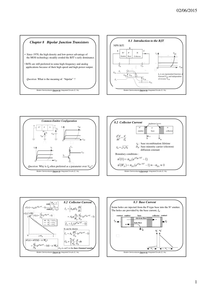
Chapter 8 Bipolar Junction Transistors
- Since 1970, the high density and low-power advantage of
the MOS technology steadily eroded the BJT’s early dominance.
- BJTs are still preferred in some high-frequency and analog
applications because of their high speed and high power output. Question: What is the meaning of “bipolar” ?
Modern Semiconductor Devices for Integrated Circuits (C. Hu) Slide 8-136
8.1 Introduction to the BJT
IC is an exponential function of forward VBE and independent
- f reverse VCB.
Modern Semiconductor Devices for Integrated Circuits (C. Hu)
NPN BJT:
N+ P N E C B
VBE VCB Emitter Base Collector
Slide 8-137
Common-Emitter Configuration Question: Why is IB often preferred as a parameter over VBE?
Modern Semiconductor Devices for Integrated Circuits (C. Hu) Slide 8-138 Modern Semiconductor Devices for Integrated Circuits (C. Hu)
8.2 Collector Current
B : base recombination lifetime DB : base minority carrier (electron) diffusion constant Boundary conditions :
N+ P N
emitter base collector
x W
depletion layers
B
Slide 8-139
It can be shown GB (s·cm4) is the base Gummel number
8.2 Collector Current
ni
2
NB
- ------e
qVBE kT
1 – n n 0
- 1
1
x/ x/WB
Modern Semiconductor Devices for Integrated Circuits (C. Hu) Slide 8-140
8.3 Base Current
Some holes are injected from the P-type base into the N+ emitter. The holes are provided by the base current, IB .
p
E' nB
'
WE WB (b)
emitter base collector contact IE
IC
electron flow
– +
hole flow IB
(a)
contact
Modern Semiconductor Devices for Integrated Circuits (C. Hu)