
SLIDE 1
1
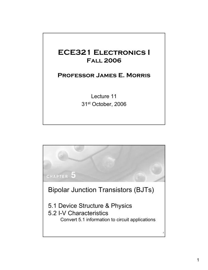
ECE321 Electronics I
Fall 2006 Professor James E. Morris
Lecture 11 31st October, 2006
2
ECE321 Electronics I Fall 2006 Professor James E. Morris Lecture - - PDF document
ECE321 Electronics I Fall 2006 Professor James E. Morris Lecture 11 31 st October, 2006 Bipolar Junction Transistors (BJTs) 5.1 Device Structure & Physics 5.2 I-V Characteristics Convert 5.1 information to circuit applications 2 1
2
Figure 5.1 A simplified structure of the npn transistor. Figure 5.2 A simplified structure of the pnp transistor.
Figure 5.3 Current flow in an npn transistor biased to operate in the active mode. (Reverse current components due to drift of thermally generated minority carriers are not shown.) Figure 5.4 Profiles of minority-carrier concentrations in the base and in the emitter of an npn transistor operating in the active mode: vBE > 0 and vCB ≥ 0.
Figure 5.5 Large-signal equivalent-circuit models of the npn BJT operating in the forward active mode. Figure 5.6 Cross-section of an npn BJT.
Figure 5.7 Model for the npn transistor when operated in the reverse active mode (i.e., with the CBJ forward biased and the EBJ reverse biased). Figure 5.8 The Ebers-Moll (EM) model of the npn transistor.
Figure 5.9 The iC –vCB characteristic of an npn transistor fed with a constant emitter current IE. The transistor enters the saturation mode of operation for vCB < –0.4 V, and the collector current diminishes. Figure 5.10 Concentration profile of the minority carriers (electrons) in the base of an npn transistor operating in the saturation mode.
Figure 5.11 Current flow in a pnp transistor biased to operate in the active mode. Figure 5.12 Large-signal model for the pnp transistor operating in the active mode.
Figure 5.13 Circuit symbols for BJTs. Figure 5.14 Voltage polarities and current flow in transistors biased in the active mode.
Figure 5.15 Circuit for Example 5.1.
Circuit for Exercise 5.10, but ignore RHS values ….. VCC= -VEE =10v, RC=5K, RE=10K, β=50 Find IE, IB, IC, VC
Figure E5.11
Circuit for Exercise 5.11: VB=1v, VE=+1.7v …….. Find α, β, VC
Figure 5.16 The iC –vBE characteristic for an npn transistor. Figure 5.17 Effect of temperature on the iC–vBE characteristic. At a constant emitter current (broken line), vBE changes by –2 mV/°C.
Figure 5.18 The iC–vCB characteristics of an npn transistor. Figure 5.21 Common-emitter characteristics. Note that the horizontal scale is expanded around the origin to show the saturation region in some detail.
Figure 5.19 (a) Conceptual circuit for measuring the iC –vCE characteristics of the BJT. (b) The iC –vCE characteristics of a practical BJT. Figure 5.20 Large-signal equivalent-circuit models of an npn BJT operating in the active mode in the common-emitter configuration.
Figure 5.21 Common-emitter characteristics. Note that the horizontal scale is expanded around the origin to show the saturation region in some detail. Figure 5.22 Typical dependence of β on IC and on temperature in a modern integrated-circuit npn silicon transistor intended for operation around 1 mA.
Figure 5.23 An expanded view of the common-emitter characteristics in the saturation region. Figure 5.24 (a) An npn transistor operated in saturation mode with a constant base current IB. (b) The iC–vCEcharacteristic curve corresponding to iB = IB. The curve can be approximated by a straight line of slope 1/RCEsat. (c) Equivalent-circuit representation of the saturated transistor. (d) A simplified equivalent-circuit model of the saturated transistor.
Figure 5.25 Plot of the normalized iC versus vCE for an npn transistor with βF = 100 and αR = 0.1. This is a plot of Eq. (5.47), which is derived using the Ebers-Moll model. Figure E5.18
Figure for Exercise 5.18: BVCBO=70v. Find VO
Table 5.3 Table 5.3 (Continued)