
SLIDE 1
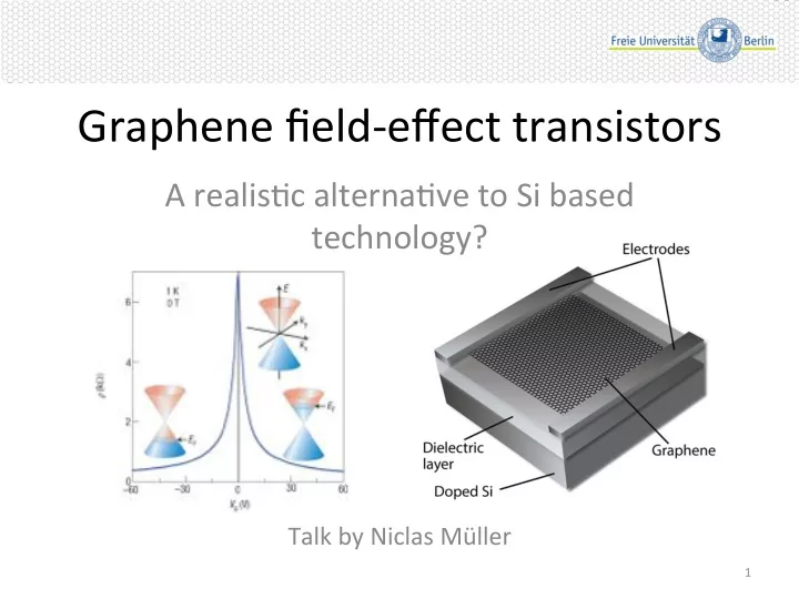
Graphene(field,effect(transistors(
A(realis4c(alterna4ve(to(Si(based( technology?( ( ( ( ( (
Talk(by(Niclas(Müller(
1(
Graphene(field,effect(transistors( - - PowerPoint PPT Presentation
Graphene(field,effect(transistors( A(realis4c(alterna4ve(to(Si(based( technology?( ( ( ( ( ( Talk(by(Niclas(Mller( 1( 1.(Introduc4on(and(Mo4va4on( Proper4es(of(field,effect(transistor(and(market(development(
1(
2( Graphene(field,effect(transistors(
Pictures(from: (F.(Schwierz,(Nature(Nanotechnology(5,(2010(
((
Important(proper4es(of(FET:(
(
((
Proper4es(of(field,effect(transistor(and(market(development(
3( Graphene(field,effect(transistors(
4( Graphene(field,effect(transistors(
Pictures(from: (Boehm(et(al.,(Anorg.(Allg.(Chem.(316,(1962( ( (Boehm(et(al.,(Carbon(24,(1986( ( ((
Reduc4on(of(graphene(oxide(by(Boehm(et(al.(in(1962(
monolyer(flakes(in(water(
((((((graphene(
5( Graphene(field,effect(transistors(
8Å( 1μm(
Pictures(from: (Novoselov(et(al.,(Science(306,(2004( ((((((((((( (Novoselov(et(al.,(Appl.(Phys.(Lea.(91,(2007(((
(
Produc4on(of(graphene(by(micromechanical(cleavage(2004(
from(graphite(
monolayer(
(
6( Graphene(field,effect(transistors(
Electrical(field(effect(in(graphene(2004(
Pictures(from: (Novoselov(et(al.,(Science(306,(2004(
( ((
7( Graphene(field,effect(transistors(
H = −t (ai,σ
+ bj,σ i, j,σ
+ bi,σ
+ aj,σ )
− # t (ai,σ
+ aj,σ i≠j,σ
+ bi,σ
+ bj,σ )
Tight,binding(hamiltonian:( Derived(energy(bands:(
E(kx,ky) = ±t 3+ f (kx,ky) + ! t ⋅ f (kx,ky)
with(
f (kx,ky) = 2cos 3kya
+ 4cos 3 2 kya = ! " # $ % &cos 3 2 kxa ! " # $ % &
Pictures(from:(Castro(Neto(et(al.,(Rev.(Mod.(Phys(81,(2009(
( ((
Bandstructure(and(ladce(
8( Graphene(field,effect(transistors(
Pictures(from:( (Castro(Neto(et(al.,(Rev.(Mod.(Phys.(81,(2009( ( (J.(Hicks,(E.H.(Corad,(MRS(Bulle4n(37,(2012((
((
rela4on:(
with(Fermi(velocity(independent(
( (vF = 3ta / 2 ≈106m / s ≈ c / 300
as(massless(rela4vis4c(par4cles( by(Dirac(equa4on(
(((
Bandstructure(and(charge,carrier(veloci4es(
9( Graphene(field,effect(transistors(
Pictures(from:( (Castro(Neto(et(al.,(Rev.(Mod.(Phys.(81,(2009( ( ((
((
with(Fermi(velocity(independent(
( (vF = 3ta / 2 ≈106m / s ≈ c / 300
Bandstructure(and(charge,carrier(veloci4es(
10( Graphene(field,effect(transistors(
Pictures(from:( (Bolo4n(et(al.,(Solid(State(Comm.(146,(2008(
((
Charge,carrier(mobility(
by(an(electric(field(E(
applying(magne4c(field:(
11( Graphene(field,effect(transistors(
Charge,carrier(mobility(
by(an(electric(field(E(
applying(magne4c(field:(
Other(materials:(
100.000cm2 /Vs 3.000.000cm2 /Vs 78.000cm2 /Vs 9.200cm2 /Vs 3.900cm2 /Vs
1.400cm2 /Vs
12( Graphene(field,effect(transistors(
Pictures(from:( (P.(Avouris(and(F.(Xia,(MRS(Bulle4n(37,(2012(
((
Characteris4cs(of(graphene(field,effect(transistors((GFETs)(
13( Graphene(field,effect(transistors(
Top,gated(GFETs(
14( Graphene(field,effect(transistors(
Top,gated(GFETs(
15( Graphene(field,effect(transistors(
Top,gated(GFETs(
16( Graphene(field,effect(transistors(
Problems:(Metal,graphene(contacts(
Effect(of(palladium(contacts(on(GFET( characteris4cs,(because(of(p,doping.( ( ! Forma4on(of(p,n,p(structure(in( graphene( ! Effect(stronger(with(decreasing(channel( length((
Pictures(from:( (P.(Avouris(and(F.(Xia,(MRS(Bulle4n(37,(2012(
((
17( Graphene(field,effect(transistors(
Problems:(Gate(dielectrics(and(substrate(
hydrophobic(
! insula4ng(materials(form(poor,
( (quality,(nonuniform(and(leaky(( ( (films((e.g.(SiO2,(HfO2,(Al2O3)(
( ! charges(trapped(at(graphene, (
( (insulator(interface(
( ! drama4c(decrease(of(carrier( (
( (mobility(
18( Graphene(field,effect(transistors(
Problems:(Gate(dielectrics(and(substrate(
(
( ( ( ( ((h,BN(
! Carrier(mobili4es((for(h,BN)(
((
( (! Scaaering(mean(free(path((
( ((for(h,BN)(
>100.000cm2 /Vs
19( Graphene(field,effect(transistors(
State(of(the(art(
Pictures(from:( (P.(Avouris(and(F.(Xia,(MRS(Bulle4n(37,(2012(
((
20( Graphene(field,effect(transistors(
State(of(the(art(
Picture(adapted(from:(( (F.(Schwierz,(Nature(Nanotech,( ( ( (nology(5,(2010((
((
21( Graphene(field,effect(transistors(
State(of(the(art(
Pictures(from:(( (F.(Schwierz,(Nature(Nanotechnology(5,(2010( ( (L.(Liao(and(X.(Duan,(Materials(Today(15,(2012((
((
22( Graphene(field,effect(transistors(
Opening(a(Band(gap:(AB,stacked(Bilayer(Graphene(
Pictures(from:(( (D.(Reddy(et(al.,(J.(Phys.:( ( (Appl.(Phys(D.(44,(2011(
((
field(
(
(! No(more(rela4vis4c(behavior(of(( ( (electrons( (! Lower(carrier(mobili4es((
23( Graphene(field,effect(transistors(
Opening(a(Band(gap:(AB,stacked(Bilayer(Graphene(
Pictures(from:(( (Zhang(et(al.,(ACS(Nano(9,(2011((
24( Graphene(field,effect(transistors(
Opening(a(Band(gap:(Graphene(nanoribbons(
Pictures(from:(( (L.P.(Biro(et(al.,(Nanoscale(4,(2012((
semiconduc4ng( metallic(
25( Graphene(field,effect(transistors(
Opening(a(Band(gap:(Graphene(nanoribbons(
Pictures(from:(( (L.P.(Biro(et(al.,(Nanoscale(4,(2012( ( (Huang(et(al.,(Mat.(Science(and(Eng.(70,(2010((
(Band(gap(inversly(propor4onal(( ((((( (to(width(of(GNR(
26( Graphene(field,effect(transistors(
Graphene(nanoribbons(–(Produc4on(methods(
Pictures(from:(( (Kosynkin(et(al.,(Nature(Leaers(458,(2009((
27( Graphene(field,effect(transistors(
Graphene(nanoribbons(–(Produc4on(methods(
Pictures(from:((L.(Jiao(et(al.,(Nature(Nanotechnology(5,(2010((
(
1.500cm2 /Vs
28( Graphene(field,effect(transistors(
Graphene(nanoribbons(–(Produc4on(methods(
Pictures(from:((J.(Bai(et(al.,(Nano(Leaers(9,(2009((
31nm( 23nm( 14nm( 9nm( 6nm(
29( Graphene(field,effect(transistors(
Graphene(nanoribbons(–(Produc4on(methods(
Pictures(from:((Li(et(al.,(Science(319,(2008((
(((((to(10.000.000(
(((((400meV(
(
((((((of((
(
((((((have(band,gap(
200cm2 /Vs
30( Graphene(field,effect(transistors(
Graphene(nanoribbons(–(Nanomeshes(
Pictures(from:((J.(Bai(et(al.,(Nature(Nanotechnology(5,(2010((
31( Graphene(field,effect(transistors(
Graphene(nanoribbons(–(Nanomeshes(
Pictures(from:((J.(Bai(et(al.,(Nature(Nanotechnology(5,(2010((
100nm( 100nm( 500nm(
32( Graphene(field,effect(transistors(
Graphene(nanoribbons(–(Nanomeshes(
Pictures(from:((J.(Bai(et(al.,(Nature(Nanotechnology(5,(2010((
graphene(nanoribbons((
500nm(
33( Graphene(field,effect(transistors(
Graphene(nanoribbons(–(Towards(industrial(applica4ons((
Pictures(from:((Sprinkle((et(al.,(Nature(Nanotechnology((5,(2010((
Etching(a(nanoscale(step( Hea4ng(to(1200°C( Further(hea4ng(to(1450°C( Fabrica4on(of(Electrodes(
up(to((
10(
2700cm2 /Vs
34( Graphene(field,effect(transistors(
Graphene(nanoribbons(–(Towards(industrial(applica4ons((
Pictures(from:(M.(Ruan(et(al.,(MRS(Bulle4n(37,(2012((
10.000(transis, tors(fabricated(
chip(
35( Graphene(field,effect(transistors(
Pictures(from: (F.(Schwierz,(Nature(Nanotechnology(5,(2010(
((