
SLIDE 1
Quantum transport in graphene L1 Disordered graphene (G) L2 - - PowerPoint PPT Presentation
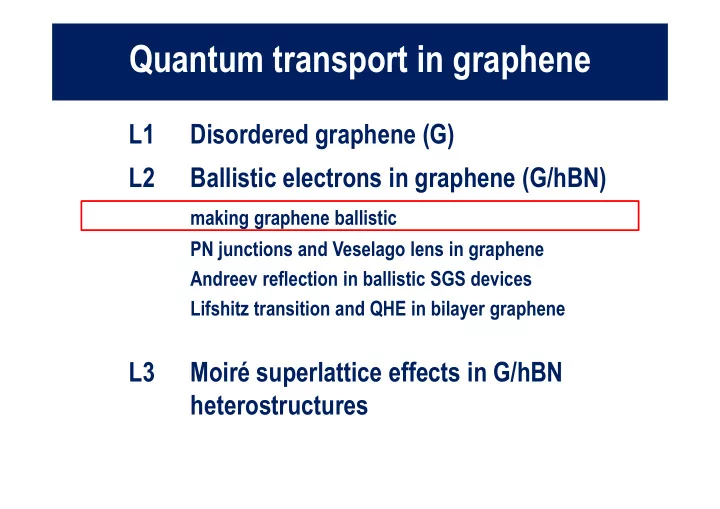
Quantum transport in graphene L1 Disordered graphene (G) L2 Ballistic electrons in graphene (G/hBN) making graphene ballistic PN junctions and Veselago lens in graphene Andreev reflection in ballistic SGS devices Lifshitz transition and QHE
Martin, Akerman, Ulbricht, Lohmann, Smet, von Klitzing, Yacoby Nature Physics 4, 144 (2008)
Cheianov, Falko, Altshuler, Aleiner PRL 99, 176801 (2007) Adam, Hwang, Galitski, Das Sarma PNAS 104, 18392 (2007)
1 2 3 4 5
2 4 6
n (1012 cm-2) (k)
graphene
300nm-SiO2/Si wafer graphene on the wafer intentionally damaged by 5 keV argon beam both samples 1x1m2 in size
Geim, Novoselov ‐ Nature Materials (2007)
n*
Scattering and charge fluctuations have same microscopic origin
long-range potentials dominate
random pseudo-magnetic field due to strain dominate disorder
random strain fluctuations
Correlation between and n* Characteristic times from weak loc.
data for graphene on SiO2, SrTiO3, hBN Couto, Costanzo, Engels, Ki, Watanabe, Taniguchi, Stampfer, Guinea, Morpurgo - PRX 4, 041019 (2014)
2nm STEM
z
hBN (‘white graphene’) sp2 – bonded insulator with a large band gap, Δ >5eV Graphene: gapless semiconductor with Dirac electrons
Yu et al - PNAS 110, 3282 (2013)
Kretinin et al - Nano Letters 14, 3270 (2014)
Taychatanapat, Watanabe, Taniguchi, Jarillo-Herrero - Nature Phys 9, 225 (2013) Lee, Wallbank, Gallagher, Watanabe, Taniguchi, Fal’ko, Goldhaber-Gordon - Science 353, 1526 (2016) Transverse magnetic focusing (caustics of skipping orbits) of ballistic electrons
) ( ) (
base
T A T A
p p v p v vp p
c
) ( p p v p v vp p
v
) (
v
p
Fermi momentum
c
p
Fermi momentum
/
2 c e c
p N vp eU
/ '
2 v h v
p N vp eU
Cheianov, VF - PR B 74, 041403 (2006) Katsnelson, Novoselov, Geim, Nature Physics 2, 620 (2006)
Cheianov, Fal’ko, Altshuler - Science 315, 1252 (2007)
c v v c
Cheianov, Fal’ko, Altshuler - Science 315, 1252 (2007)
Heersche et al ‐ Nature Physics (2007)
Heersche et al - Nature 446, 56-59 (2007)
F
h e
graphene N-doped by S-cond metal
graphene N-doped by S-cond metal N-type graphene with low density set by gates
graphene N-doped by S-cond metal
N-type graphene with low density set by gates 2e
graphene N-doped by S-cond metal P-type graphene with low density set by gates
2e
Ben-Shalom, Zhu, Fal’ko, Mishchenko, Kretinin, Novoselov, Woods, Watanabe, Taniguchi, Geim, Prance Nature Physics 12, 318 (2016) Ballistic graphene: Fabry-Perot
at T>Tc
p-n-p regime
Ballistic SGS: Fabry-Perot oscillations of critical supercurrent current at T<Tc
random caustics of retracing Andreev paths near a disordered edge
2
B
1
B
Meier, Fal’ko, Glazman – PRB 93, 184506 (2016)
2
Ben Shalom, Zhu, Fal’ko, Mishchenko, Kretinin, Novoselov, Woods, Watanabe, Taniguchi, Geim, Prance Nature Physics 12, 318 (2016)
Cooper pair transfer via non-retracing Andreev paths (e-h loops) d ev ~
1
B random caustics of retracing Andreev paths near a disordered edge (up to
Calado, Goswami, Nanda, Diez, Akhmerov, Watanabe, Taniguchi, Klapwijk, Vandersypen Nature Nanotechnology 10, 761 (2015) Delft flux qubit
Lancaster graphene FET-based SQUID: supercurrent can be switched on/off fast using electrostatic gates: quantum device for magnetic field measurement
graphene N-doped by S-cond metal graphene with ne=0
2e
Beenakker - PRL 97, 067007 (2006)
Efetov, Wang, Handschin, Efetov, Shuang, Cava, Taniguchi, Watanabe, Hone, Dean, Kim Nature Physics 12, 328-332 (2016)
1
3
skew inter-layer
A
hopping B ~
McCann, Fal’ko ‐ PRL 96, 086805 (2006)
v a v 1 . ~ 2 3
3 3
i y x
2 1 1 1 2 1 2 1 3 3 2 1
z
Dirac point generates a 4-fold degenerate ε=0 Landau level
McClure ‐ PR 104, 666 (1956)
descending/raising
8-fold degenerate ε=0 Landau level, which splits when inversion symmetry is broken and
McCann, VF ‐ PRL 96, 086805 (2006)
e m m 05 . ~B
c
e
m m 035 .
1
y x y x z c e
ip p ip p l B A rot A i p
; ,
1eV
Zhang, et al - Nature 459, 820 (2009)
(Rotenberg’s group at Berkeley NL) Oostinga, et al - Nature Mat 7, 151 (2008)
conductance and ferromagnetic quantum Hall states
1
3
skew inter-layer
A
hopping B ~
McCann, Fal’ko ‐ PRL 96, 086805 (2006)
v a v 1 . ~ 2 3
3 3
i y x
2 1 1 1 2 1 2 1 3 3 2 1
z
v v u u F
u
3 1 1
2 ) ( 1
2 2 1 2 1
meV v v u 14 ~ 8
1 3
F 2 1
v v u u F
3 1 1
2 2 1 2 1
v v u u F
u
3 1 1
2 ) ( 1
2 2 1 2 1
F 2 1
v v u u F
3 1 1
2 2 1 2 1
3
Ilya Lifshitz 1917‐1982 Kharkov/Moscow
] [Tesla B ] [eV E
2 1 1 1 2 1 2 1 3 3 2 1
] [Tesla B ] [eV E
] [Tesla B ] [eV E
] [Tesla B
] [eV E
Varlet, Bischoff, Simonet, Watanabe, Taniguchi, Ihn, Ensslin, Mucha‐Kruczyński, Fal’ko ‐ PRL 113, 116602 (2014)
2nm STEM
Ponomarenko, Geim, Zhukov, Jalil, Morozov, Novoselov, Grigorieva, Hill, Cheianov, Fal’ko, Watanabe, Taniguchi, Gorbachev Nature Physics 7,958 (2011)
Insulating state in closely gated graphene at n=0