
SLIDE 1
Quantum Transport of Quantum Quantum Transport of Transport of
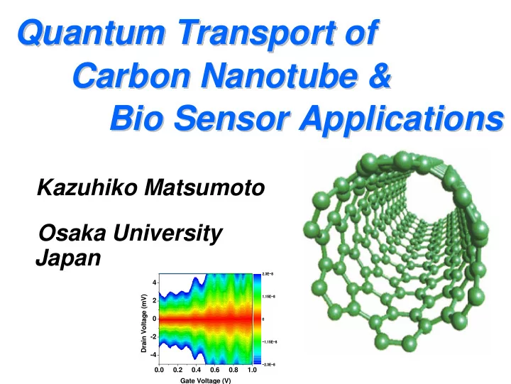
0.0 0.2 0.4 0.6 0.8 1.0
- 4
- 2
2 4 Gate Voltage (V) Drain Voltage (mV)
- 2.3E-8
- 1.15E-8
1.15E-8 2.3E-8
Quantum Transport of Transport of Quantum Transport of Quantum - - PowerPoint PPT Presentation
Quantum Transport of Transport of Quantum Transport of Quantum Carbon Nanotube Nanotube & & Carbon Bio Sensor Applications Bio Sensor Applications Kazuhiko Matsumoto Osaka University Japan 2.3E-8 4 Drain Voltage (mV) 1.15E-8
0.0 0.2 0.4 0.6 0.8 1.0
2 4 Gate Voltage (V) Drain Voltage (mV)
1.15E-8 2.3E-8
15 20 25 30 35 40 45 50
Gate Voltage (V)
Carbon Nanoatube Source Drain 73nm 1~2 nm ~3 nm Si Aptamer Aptamer SiO2 Deby Deby Length Length IgE IgE
50 100 150 Gate Voltage (V) Drain Voltage (mV)
5E-6 1E-5
d2ID/dVD
2
Back gate n+-Si SiO2 SiNx CNT Source Drain Catal yst Water proof resist
20 40 60 80 100 dID/dVD (S) Gate Voltage (V) Drain Voltage (mV)
4E-7 9E-7 1.4E-6 1.9E-6 2.4E-6 2.9E-6 3.4E-6 3.9E-6 4E-6
Back Gate Si Sub. SiO2 Drain Source Back Gate Si Sub. SiO2 Drain
Drain EF Source CNT h+ e/C EF
Quantum Well
Back Gate Si Sub. SiO2 Drain Source Back Gate Si Sub. SiO2 Drain
VG A VD=11 mV ID
Drain
EF
Source CNT
EF
Carbon Nanoatube Drain Source 73nm
Gate Voltage VG (V) 10 20 30 40 50
10 20 7.3 K VD=11 mV
T >>h/e2 =25.8kΩ≡ R Q
T <<e2 /2C
T
(Charging Energy) h+ Drain Source Tunnel Res. RT>> Quantum Res. RQ
10 20 30 40 50
1 0 2 0 7.3 K VD=11 mV ΔVG=3V
E F Drain E F Source CNT h+ e/C
Drain Source
h+ Drain Source Tunnel Res. RT>> Quantum Res. RQ
10 20 30 40 50
1 0 2 0 7.3 K VD=11 mV ΔVG=3V
E F Drain E F Source CNT h+ e/C
Drain Source
10 20 30 40 50
Gate Voltage (V)
Carbon Nanoatube Source Drain 73nm
Back Gate Si Sub. SiO2 Drain Source Back Gate Si Sub. SiO2 Drain
VG A VD=11 mV
EF
Drain
EF
Source CNT
ID
10 20 30 40 50
Gate Voltage (V)
15 20 25 30 35 40 45 50
Gate Voltage (V)
ΔVG=0.65 V
Gate Electrode
4μm
SiO2 Drain Source
ΔEQ Discrete Energy Level
Hole
73nm
15 20 25 30 35 40 45 50
Gate Voltage (V)
ΔVG=0.65 V
EF
Drain
EF
Source CNT
Coulmb Gap Quantum Level
15 20 25 30 35 40 45 50
Gate Voltage (V)
ΔVG=0.65 V
ΔVG=0.65 V
0.05 0.1 0.15 0.2
20 40 Gate Voltage (V) 7.2 K
0.04 0.06 0.08 0.1 0.12 0.14 0.16 0.18
Gate Voltage (V) 7.3 K Drain current (nA)
0.04 0.06 0.08 0.1 0.12 0.14 0.16 0.18
Gate Voltage (V) 7.3 K Drain current (nA) Gate Electrode
4μm
SiO2 Drain Source
ΔEQ Discrete Energy Level
Hole
73nm
F Q
SEM Observation
Calculated
h+ Drain Source
0.04 0.06 0.08 0.1 0.12 0.14 0.16 0.18
Gate Voltage (V) 7.3 K
Tunnel Res. RT<< Quantum Res. RQ
EF EF
Drain CNT
h +
Source
Drain Source
ε π ε π
2 2 2 2
4 T e e G
R L R L
h h = Γ + Γ + Γ Γ =
E F E F Drain CNT h+ Source
R L Γ
R L R L
E F E F Drain CNT h+ Source
R L Γ
Drain Source
h+ Drain Source
h+ Drain Source CNT CNT
h+ Drain Source
0.04 0.06 0.08 0.1 0.12 0.14 0.16 0.18
Gate Voltage (V) 7.3 K
Tunnel Res. RT<< Quantum Res. RQ
EF EF
Drain CNT
h +
Source
h+ Drain Source
h+ Drain Source
Tunnel Res. RT>> Quantum Res. RQ
15 20 25 30 35 40 45 50
Gate Voltage (V)
10 20 30 40 50
1 0 2 0 7.3 K VD=11 mV ΔVG=3V
Tunnel Res. RT ~ Quantum Res. RQ
E F Drain E F Sourc e CNT h+ e/C E F Drain E F Source CNT h+ e/C
15 20 25 30 35 40 45 50
Gate Voltage (V)
Carbon Nanoatube Source Drain 73nm 1~2 nm ~3 nm Si Aptamer Aptamer SiO2 Deby Deby Length Length IgE IgE
50 100 150 Gate Voltage (V) Drain Voltage (mV)
5E-6 1E-5
d2ID/dVD
2
Back gate n+-Si SiO2 SiNx CNT Source Drain Catal yst Water proof resist
20 40 60 80 100 dID/dVD (S) Gate Voltage (V) Drain Voltage (mV)
4E-7 9E-7 1.4E-6 1.9E-6 2.4E-6 2.9E-6 3.4E-6 3.9E-6 4E-6
窓(100 μm×100 μm)
Back gate n+-Si SiO2 SiNx CNT Source Drain Catalyst Water proof resist
SEM image of top-gate
immobilized a-PSA.
a-PSA 100 nm
Top-gate with a-PSA
Drain V (V)
0.0 0.2 0.4 0.6 0.8 1.0 500 1000 1500
Top Gate
Electron Current
Ag/AgCl Gate
Back Gate Source Top Gate SiO2 n+-Si SiNx CNT Analyzer Drain Antibody a-PSA Antigen PSA
30th, August, 2006 第67回応用物理学会学術講演会 30p-D-17
Drain Voltage: +1 V Top-gate Voltage: +1 V Back-gate Voltage: +5 V 2 10-9 4 10-9 6 10-9 8 10-9 1 10-8 1 10 100 1000 104 105
(VD = 1V, VBG = +5 V)
15th, September, 2006 SSDM, C-8-2
Where
PSA Cons.[nmol/L]
15th, September, 2006 SSDM, C-8-2
Antigen Antibody
Source Drain Sensing Area 1.5 μm 6 μm
2 10-9 4 10-9 6 10-9 8 10-9 1 10-8 1.2 10-8
0.1 10 103
Back-gate
n+-Si SiO2 SiNx CNT
Source
Drain
Resist
Langmuir Equation Na / Ntotal = Keq CPSA / (1+Keq CPSA )
Antigen Antibody
PSA Conc. (nM) NO gate metal With gate metal
5 10 15 20 25 30 35 0.1 1 10 100 103 104
VD = + 1 VTG = + 1 V VBG = + 5 V
100 200 300 400 10 20 I DS(nA) Time (min) 0.25 nM 2.2 nM 18.5 nM 159 nM
Carbon Carbon Nanotube Nanotube
金属電極 金属電極
1~2 nm ~3 nm Si Aptamer Aptamer SiO2 Deby Deby Length Length
IgE IgE
4μm
CNT aptamer IgE
100 200 10 12 14 16 18 Time (min) ISD (nA) IgE VD = 0.2 V VG = 0 V
Arrows indicate the point of adding IgE IgE solutions.
1 8 8 −
50 100 150 5 10
V VDS
DS=
=200 mV 200 mV V VGS
GS=
=0 V 0 V
100 101 2 3 4 5 IgE concentration (nM) Δ ISD (nA)
CNT aptamer IgE
100 200 10 12 14 16 18 Time (min) ISD (nA) IgE VD = 0.2 V VG = 0 V
250 pM 250 250 pM pM 2.2 nM 2.2 2.2 nM nM 18.5 nM 18.5 18.5 nM nM
100 200 10 12 14 16 18 Time (min) ISD (nA) IgE VD = 0.2 V VG = 0 V
250 pM 250 250 pM pM 2.2 nM 2.2 2.2 nM nM 18.5 nM 18.5 18.5 nM nM
2002, 74, 4488-4495
2004, 76, 5230-5235
12
Back gate in Air 107 ~85 mV/dec ~210 mV/dec Top gate in Liquid 107 subthreshold slope
transconductance ~100 μS/μm
(Vds=100 mV)
~700 μS/μm (Vds=100 mV)
500 1000 1E-14 1E-13 1E-12 1E-11 1E-10 1E-9 1E-8 1E-7
Vd=100 mV
back gate in air top gate in PBS
Drain Source Reference top gate Si Substrate SiO2 CNT back gate Resist 10 mM PBS
Plane CNT Experiment
103 1 10-15 10-12 10-9 10-6 10-3 106
ts ~ Ns
2
D 1 ρ0
2
ts ~ Nsa0 D 1 ρ0
5 nmol/L
0.1 pmol/L
15 20 25 30 35 40 45 50
Gate Voltage (V)
Carbon Nanoatube Source Drain 73nm 1~2 nm ~3 nm Si Aptamer Aptamer SiO2 Deby Deby Length Length IgE IgE
50 100 150 Gate Voltage (V) Drain Voltage (mV)
5E-6 1E-5
d2ID/dVD
2
Back gate n+-Si SiO2 SiNx CNT Source Drain Catal yst Water proof resist
20 40 60 80 100 dID/dVD (S) Gate Voltage (V) Drain Voltage (mV)
4E-7 9E-7 1.4E-6 1.9E-6 2.4E-6 2.9E-6 3.4E-6 3.9E-6 4E-6