overview ece 553 testing and
play

Overview ECE 553: TESTING AND Definition Ad-hoc methods - PDF document

11/11/2014 Overview ECE 553: TESTING AND Definition Ad-hoc methods TESTABLE DESIGN OF Scan design DIGITAL SYSTEMS DIGITAL SYSTEMS Design rules D i l Scan register Scan flip-flops Scan test sequences


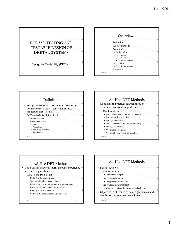
  1. 11/11/2014 Overview ECE 553: TESTING AND • Definition • Ad-hoc methods TESTABLE DESIGN OF • Scan design DIGITAL SYSTEMS DIGITAL SYSTEMS – Design rules D i l – Scan register – Scan flip-flops – Scan test sequences – Overhead Design for Testability (DFT) - 1 – Scan design system • Summary 11/11/2014 2 Definition Ad-Hoc DFT Methods • Good design practices learned through • Design for testability (DFT) refers to those design experience are used as guidelines: techniques that make test generation and test – Don’t-s and Do-s application cost-effective. • Avoid asynchronous (unclocked) feedback. • DFT methods for digital circuits: • DFT methods for digital circuits: • Avoid delay dependant logic. – Ad-hoc methods • Avoid parallel drivers. – Structured methods: • Avoid monostables and self-resetting logic. • Scan • Avoid gated clocks. • Partial Scan • Built-in self-test (BIST) • Avoid redundant gates. • Boundary scan • Avoid high fanin fanout combinations. 11/11/2014 3 11/11/2014 4 Ad-Hoc DFT Methods Ad-Hoc DFT Methods • Good design practices learnt through experience • Design reviews are used as guidelines: – Manual analysis – Don’t-s and Do-s (contd.) • Conducted by experts. – Programmed analysis g y • Make flip-flops initializable. • Separate digital and analog circuits. • Using design auditing tools • Provide test control for difficult-to-control signals. – Programmed enforcement • Buses can be useful and make life easier. • Must use certain design practices and cell types. • Limit gate fanin and fanout. • Objective: Adherence to design guidelines and • Consider ATE requirements (tristates, etc.) testability improvement techniques. 11/11/2014 5 11/11/2014 6 1
  2. 11/11/2014 Ad-Hoc DFT Methods Scan Design • Disadvantages of ad-hoc DFT methods: – Objectives • Experts and tools not always available. • Simple read/write access to all or subset of storage • Test generation is often manual with no guarantee of elements in a design. high fault coverage. • Direct control of storage elements to an arbitrary value • Direct control of storage elements to an arbitrary value • Design iterations may be necessary. (0 or 1). • Direct observation of the state of storage elements and hence the internal state of the circuit. Key is – Enhanced controllability and observability. 11/11/2014 7 11/11/2014 8 Scan Design Scan Design Rules – Circuit is designed using pre-specified design rules. – Test structure (hardware) is added to the verified design: • Use only clocked D-type flip-flops for all state • Add one (or more) test control (TC) primary input. variables. • Replace flip-flops by scan flip-flops and connect to form one or more shift registers in the test mode. registers in the test mode. • At least one PI pin must be available for test; more • At least one PI pin must be available for test; more • Make input/output of each scan shift register controllable/observable from pins, if available, can be used. PI/PO. • All clocks must be controlled from PIs. – Use combinational ATPG to obtain tests for all testable faults in the combinational logic. • Clocks must not feed data inputs of flip-flops. – Add shift register tests and convert ATPG tests into scan sequences for use in manufacturing test. 11/11/2014 9 11/11/2014 10 Scan Flip-Flop (master-slave) Correcting a Rule Violation Master latch Slave latch D • All clocks must be controlled from PIs. TC Q Logic Comb. overhead logic D1 Q MUX Q SD Comb. FF D2 logic logic CK CK D flip-flop Comb. Master open Slave open CK logic t Q D1 Comb. FF Normal mode, D selected Scan mode, SD selected D2 TC logic t CK 11/11/2014 11 11/11/2014 12 2

  3. 11/11/2014 Level-Sensitive Scan-Design Latch Adding Scan Structure (LSSD) Master latch Slave latch PI PO D Q SFF SCANOUT Combinational MCK Q logic logic SFF SFF SCK D flip-flop SFF SD Normal MCK mode Logic TCK overhead MCK TCK Scan mode Not show n: CK or TC or TCK TCK MCK/SCK feed all SCANIN SFFs (scan Flip- SCK t flops). 11/11/2014 13 11/11/2014 14 Comb. Test Vectors Comb. Test Vectors Don’t care or random PI I1 I2 bits SCANIN S1 S2 PI I1 I2 O2 PO O1 TC 0 0 0 0 0 0 0 1 0 0 0 0 0 0 0 1 0 0 0 0 0 0 0 Combinational SCANIN SCANOUT TC logic PO O1 O2 Next Presen S2 N1 N2 S1 state t SCANOUT N1 N2 state Sequence length = ( n sff + 1) n comb + n sff clock periods n comb = number of combinational vectors n sff = number of scan flip-flops 11/11/2014 15 11/11/2014 16 Multiple Scan Registers Testing Scan Register • Scan flip-flops can be distributed among any • Scan register must be tested prior to application of scan test number of shift registers, each having a separate sequences. scanin and scanout pin. • A shift sequence 00110011 . . . of length n sff +4 in scan • Test sequence length is determined by the longest mode (TC=0) produces 00, 01, 11 and 10 transitions in all flip-flops and observes the result at SCANOUT output. scan shift register. g • Total scan test length: • Just one test control (TC) pin is essential. PI/SCANIN PO/ Combinational (( n sff + 1) n comb + n sff ) + ( n sff + 4) clock periods . SCANOUT M logic U ( n comb + 2) n sff + n comb + 4 clock periods . SFF X • Example: 2,000 scan flip-flops, 500 comb. vectors, total SFF scan test length ~ 10 6 clocks. SFF • Multiple scan registers reduce test length. TC CK 11/11/2014 17 11/11/2014 18 3

  4. 11/11/2014 Hierarchical Scan Scan Overhead • Scan flip-flops are chained within subnetworks • IO pins: One pin necessary. before chaining subnetworks. • Area overhead: • Advantages: – Gate overhead = [4 n sff /( n g +10 n ff )] x 100%, • Automatic scan insertion in netlist where n g = comb. gates ; n ff = flip-flops ; • Circuit hierarchy preserved – helps in debugging and design • Example – n g = 100k gates, n ff = 2k flip-flops , overhead = 6.7%. p g , f p f p , changes g g ff – More accurate estimate must consider scan wiring and layout • Disadvantage: Non-optimum chip layout. area. Scanin Scanout • Performance overhead: SFF1 SFF4 SFF1 SFF3 – Multiplexer delay added in combinational path; approx. two Scanin gate-delays. Scanout SFF2 SFF3 – Flip-flop output loading due to one additional fanout; approx. SFF4 SFF2 5-6%. Hierarchical netlist Flat layout 11/11/2014 19 11/11/2014 20 Optimum Scan Layout Scan Area Overhead X’ Linear dimensions of active area: X X = (C + S) / r SFF IO y = track dimension, w ire X’ = (C + S + α S) / r cell pad w idth+separation Y’ = Y + ry = Y + Y(1-- β ) / T C = total comb. cell w idth S = total non-scan FF cell SCANIN Flip- Area overhead w idth flop s = fractional FF cell area X Y X’Y’--XY XY cell ll = S/(C+S) = -------------- x 100% Y Y’ α = SFF cell w idth fractional XY increase 1-- β r = number of cell row s TC SCAN or routing channels = [ (1+ α s) ( 1+ ------- ) – 1 ] x 100% OUT β = routing fraction in active T area T = cell height in track dimension y 1-- β Routing channels = ( α s + ------- ) x 100% Active areas: XY and X’Y’ Interconnects T 11/11/2014 21 11/11/2014 22 Example: Scan Layout ATPG Example: S5378 • 2,000-gate CMOS chip • Fractional area under flip-flop cells, s = 0.478 Original Full-scan • Scan flip-flop (SFF) cell width increase, α α = 0.25 • Routing area fraction, β β = 0.471 Number of combinational gates 2,781 2,781 Number of non-scan flip-flops (10 gates each) 179 0 • Cell height in routing tracks, T = 10 Number of scan flip-flops (14 gates each) 0 179 Gate overhead 0.0% 15.66% • Calculated overhead = 17 24% • Calculated overhead = 17.24% Number of faults 4,603 4,603 • Actual measured data: PI/PO for ATPG 35/49 214/228 70.0% 99.1% Fault coverage 70.9% 100.0% Fault efficiency Scan implementation Area overhead Normalized clock rate ______________________________________________________________________ Number of ATPG vectors 414 585 Scan sequence length 414 105,662 None 0.0 1.00 Hierarchical 16.93% 0.87 Optimum layout 11.90% 0.91 11/11/2014 23 11/11/2014 24 4

Download Presentation
Download Policy: The content available on the website is offered to you 'AS IS' for your personal information and use only. It cannot be commercialized, licensed, or distributed on other websites without prior consent from the author. To download a presentation, simply click this link. If you encounter any difficulties during the download process, it's possible that the publisher has removed the file from their server.

Recommend


More recommend