Overview Motivation About the Course and the Instructor ECE 553: - - PDF document

overview
SMART_READER_LITE
LIVE PREVIEW

Overview Motivation About the Course and the Instructor ECE 553: - - PDF document

8/14/2014 Overview Motivation About the Course and the Instructor ECE 553: TESTING AND Conduct TESTABLE DESIGN OF Outline Coursepack DIGITAL SYSTES DIGITAL SYSTES Introduction VLSI realization process


slide-1
SLIDE 1

8/14/2014 1

ECE 553: TESTING AND TESTABLE DESIGN OF DIGITAL SYSTES DIGITAL SYSTES

Motivation and Introduction

Overview

  • Motivation
  • About the Course and the Instructor

– Conduct – Outline – Coursepack

8/14/2014 2

  • Introduction

– VLSI realization process – Contract between design house and fab vendor – Test v/s verification – Need for testing: doing business, ideal v/s real testing – Levels of testing – rule of 10 (or 20) – Cost of manufacturing

Motivation

  • Where do the manufacturing $ go?
  • Overhead of one or two photomicrographs

– What is test on a chip?

8/14/2014 3

  • Course conduct

– Your responsibilities and mine

  • Course outline
  • Course material information

– References and reading material

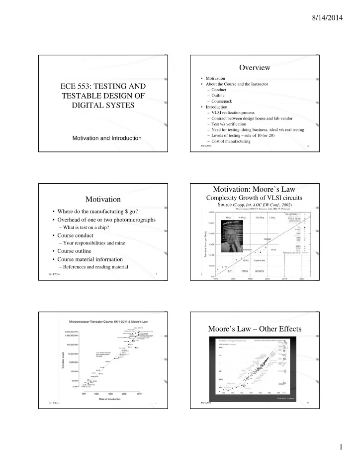
Motivation: Moore’s Law

Complexity Growth of VLSI circuits

Source (Copp, Int. AOC EW Conf., 2002)

8/14/2014 4 8/14/2014 5

Moore’s Law – Other Effects

8/14/2014 6

slide-2
SLIDE 2

8/14/2014 2

Thermal Effect of Moore’s law

 Moore’s law

Greater packaging densities Higher power densities

8/14/2014 7

Higher temperature

 Effects

Reliability Performance Power Cooling cost Introduction: Challenges under deep submicron technologies (Yao)

Chip size decreases Power density increases

Source: Intel Source: Intel

Power density increases Leakage power make it worse Chip becomes hotter

Source: Wang et al. ISPD2003

Microprocessor Cost per Transistor

Cost of testing will EXCEED cost of design/manufacturing (Source: ITR-Semiconductor, 2002)

8/14/2014 9

VLSI Realization Process

Determine requirements Write specifications D i th i d V ifi ti Customer’s need

8/14/2014 10

Design synthesis and Verification Fabrication Manufacturing test Chips to customer Test development

Technology Directions: SIA Roadmap

Year 1999 2002 2005 2008 2011 2014 Feature size (nm) 180 130 90 45 32 22 Mtrans/cm2 7 14-26 47 115 284 701 Chi i (

2)

170 170 214 235 269 308 354

Present and Future

Chip size (mm2) 170 170-214 235 269 308 354 Signal pins/chip 768 1024 1024 1280 1408 1472 Clock rate (MHz) 600 800 1100 1400 1800 2200 Wiring levels 6-7 7-8 8-9 9 9-10 10 Power supply (V) 1.8 1.5 1.2 0.9 0.6 0.6 High-perf power (W) 90 130 160 170 174 183 Battery power (W) 1.4 2.0 2.4 2.0 2.2 2.4

http://www.itrs.net/ntrs/publntrs.nsf

Contract between a design house and a fab vendor

  • Design is complete and checked (verified)
  • Fab vendor: How will you test it?
  • Design house: I have checked it and …
  • Fab vendor: But, how would you test it?

8/14/2014 12

  • Desing house: Why is that important? It is between

I and my clients – it is none of your business

  • Fab vendor – Sorry you can take your business

some where else. complete the story and determine the reasons for the importance of test generation etc.

slide-3
SLIDE 3

8/14/2014 3

Contract between design …

Hence:

  • “Test” must be comprehensive
  • It must not be “too long”

Issues:

8/14/2014 13

Issues:

  • Model possible defects in the process

– Understand the process

  • Develop logic simulator and fault simulator
  • Develop test generator
  • Methods to quantify the test efficiency

Verification v/s Testing

Definitions

  • Design synthesis: Given an I/O function, develop a

procedure to manufacture a device using known materials and processes.

8/14/2014 14

  • Verification: Predictive analysis to ensure that the

synthesized design, when manufactured, will perform the given I/O function.

  • Test: A manufacturing step that ensures that the physical

device, manufactured from the synthesized design, has no manufacturing defect.

Verification v/s Testing

  • Verifies correctness of

design.

  • Performed by simulation,

hardware emulation, or formal methods

  • Verifies correctness of

manufactured hardware.

  • Two-part process:

– 1. Test generation: software process executed once during design

8/14/2014 15

formal methods.

  • Performed once prior to

manufacturing.

  • Responsible for quality of

design.

executed once during design – 2. Test application: electrical tests applied to hardware

  • Test application performed on

every manufactured device.

  • Responsible for quality of devices.

Need for testing

  • Functionality issue

– Does the circuit (large or small) work?

  • Density issue

– Higher density  higher failure probability

8/14/2014 16

  • Application issue

– Life critical applications

  • Maintenance issue

– Need to identify failed components

  • Cost of doing business
  • What does testing achieve?

– Discard only the “bad product”? – see next three slides

Problems of Ideal Tests

  • Ideal tests detect all defects produced in the

manufacturing process.

  • Ideal tests pass all functionally good devices

8/14/2014 17

  • Ideal tests pass all functionally good devices.
  • Very large numbers and varieties of possible

defects need to be tested.

  • Difficult to generate tests for some real defects.

Defect-oriented testing is an open problem.

Real Tests

  • Based on analyzable fault models, which may not

map on real defects.

  • Incomplete coverage of modeled faults due to high

complexity

8/14/2014 18

complexity.

  • Some good chips are rejected. The fraction (or

percentage) of such chips is called the yield loss.

  • Some bad chips pass tests. The fraction (or

percentage) of bad chips among all passing chips is called the defect level.

slide-4
SLIDE 4

8/14/2014 4

Testing as Filter Process

Good chips Prob(good) = y Prob(pass test) = high Mostly good chips

8/14/2014 19

Fabricated chips Defective chips Prob(bad) = 1- y Prob(fail test) = high Mostly bad chips

Levels of testing (1)

  • Levels

– Chip – Board – System

8/14/2014 20

y

  • Boards put together
  • System-on-Chip (SoC)

– System in field

  • Cost – Rule of 10

– It costs 10 times more to test a device as we move to higher level in the product manufacturing process

Levels of testing (2)

  • Other ways to define levels – these are important

to develop correct “fault models” and “simulation models”

– Transistor G t

8/14/2014 21

– Gate – RTL – Functional – Behavioral – Architecture

  • Focus: Chip level testing – gate level design

Cost of Testing

  • Design for testability (DFT)

– Chip area overhead and yield reduction – Performance overhead

  • Software processes of test

8/14/2014 22

– Test generation and fault simulation – Test programming and debugging

  • Manufacturing test

– Automatic test equipment (ATE) capital cost – Test center operational cost

Cost of Manufacturing Testing in 2010+

  • 0.5-1.0GHz, analog instruments,1024 digital pins:

ATE purchase price

– = $4.0M + 1,024 x $5,000 = $9.12M

  • Running cost (five-year linear depreciation)

8/14/2014 23

Running cost (five year linear depreciation)

– = Depreciation + Maintenance + Operation – = $1.80M + $0.185M + $1.5M – = $3.485M/year

  • Test cost (24 hour ATE operation)

– = $3.485M/(365 x 24 x 3,600) – = 11.05 cents/second

Roles of Testing

  • Detection: Determination whether or not the device

under test (DUT) has some fault.

  • Diagnosis: Identification of a specific fault that is

present on DUT.

8/14/2014 24

  • Device characterization: Determination and

correction of errors in design and/or test procedure.

  • Failure mode analysis (FMA): Determination of

manufacturing process errors that may have caused defects on the DUT.

slide-5
SLIDE 5

8/14/2014 5

Summary

  • About the course
  • Expectations
  • Why test?

8/14/2014 25

  • Cost issue – First look