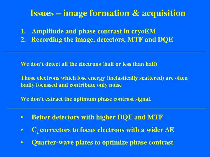
SLIDE 1 Issues – image formation & acquisition
1. Amplitude and phase contrast in cryoEM
- 2. Recording the image, detectors, MTF and DQE
We don’t detect all the electrons (half or less than half) Those electrons which lose energy (inelastically scattered) are often badly focussed and contribute only noise We don’t extract the optimum phase contrast signal.
- Better detectors with higher DQE and MTF
- Cc correctors to focus electrons with a wider ΔE
- Quarter-wave plates to optimize phase contrast
SLIDE 2 Ultramicroscopy (1988) 25, 279-292 See also Toyoshima et al, Ultramicroscopy (1993) 48, 165-176 120kV – 5.8% 200kV – 4.8%
(at 120kV)
SLIDE 3 Toyoshima & Unwin, Ultramicroscopy 1988
SLIDE 4
SLIDE 5
100 keV electron scattering factors (IAM) |f| η per atom H 0.63 0.008 C 2.90 0.037 N 2.57 0.045 O 2.34 0.052 S 6.08 0.08 U 22 0.22 Understanding images of unstained biological molecules
SLIDE 6
100 keV electron scattering factors (IAM) |f| η per atom H 0.63 0.008 C 2.90 0.037 N 2.57 0.045 O 2.34 0.052 S 6.08 0.08 U 22 0.22 Some problems in understanding images of unstained biological molecules
SLIDE 7
Embedding in ice
Ratio of amplitude to phase contrast η(p-w) = (fp ηp – fw ηw)/(fp-fw) = ηp + (fw/(fp-fw)).(ηp – ηw)
SLIDE 8 |f|/mol
moles |f|/Å3 η estimated density
/Å3 “fudge” from used M.W. bonding (g/cc) 18 H2O (ice) 3.6 0.033 0.12 0.036 0.13 0.03 1.0 108.5 protein (lo dose) 25.7 0.008 0.198 0.035 0.18 0.04 1.4 protein (hi dose) ~13 ~0.008 ~0.10 ~0.04 ~0.10 ~0.04 0.7 376 UA (lo dose) 48.7 0.0048 0.23 0.12 0.22 0.14 3.0 ~300 UA (hi dose) ~35 ~0.006 ~0.21 ~0.17 ~0.21 ~0.17 3.0 UA - prot (lo dose) -
0.64 0.05 0.48
- UA - prot (hi dose) -
- ~0.11
~0.27 ~0.11 ~0.27
0.035 0.05 0.066 Note: for high dose images of negatively stained specimens, a 50% mass loss of organic matter has been assumed compared with low does images.
SLIDE 9
Detectors for Electron Microscopy
Film (SO-163) Phosphor/Fibre Optics/cooled CCD Phosphor/Lens/cooled CCD Hybrid Pixel Detectors (Medipix) Monolithic Active Pixel Sensors (MAPS/CMOS)
SLIDE 10
Monte Carlo simulation of electron trajectories in silicon Detector thickness = 300 microns, pixel=55 microns Extension of simulations to include energy deposition (GM)
SLIDE 11
SLIDE 12 Optical Density Vacuum 1.00 Beryllium 1.13 Plastic film 1.19 Aluminium 1.35 Silicon 1.38 Copper 1.55
Backscattering test – film loaded upside down above test materials
SLIDE 13
Gatan Ultrascan 4000
SLIDE 14 from Booth et al (2004) JSB, 147, 116-127.
Gatan US4000 CCD camera versus Kodak SO-163 film for 200keV electrons
film better ---> CCD better Gatan US4000 SO-163 film
Gatan US4000 SO-163 film
SLIDE 15
Medipix 2
SLIDE 16 MediPix 2
hybrid pixel sensor
Campbell et al at CERN
- r electron gun
- r electrons
SLIDE 17 Single pixel schematic
(Silicon/CdTe)
SLIDE 18 Image of grid with 18 electrons/pixel No counts are recorded in areas not exposed to incident electrons Image with < 0.01 electron/pixel Electrons are almost all recorded in
Medipix 2 - grid shadow
SLIDE 19
Mean Intensity 111 Std Deviation 11 Mean Intensity 4.7 Std Deviation 1.8 Film exposure equivalent to above Mean Intensity 116 spots not visible, unmeasurable Std Deviation 24
Medipix 2 - raster of spots
SLIDE 20
120keV electrons/45keV threshold 300keV electrons/80keV threshold
SLIDE 21
120keV electrons; a-c ΔE=80keV, a-g 40keV, a-j 20keV, a-n >0.5%, o - rare
SLIDE 22 Resolution of Quad_Medipix2 from 120 – 300 keV
300 mesh grid, spacing ~650 microns in image
SLIDE 23 10 sec blank 30 minute cosmics 800 el/pixel shadow Cs137 β low (scale 0-5) Cs137 β med Cs137 β high
SLIDE 24
SLIDE 25 Some DQE formulae DQE(0) = (S/Nout)2 / (S/Nin)2
DQE(0) = (Σipi)2 / (Σi2pi)
(where pi is probablility of recording a single incident electron in i pixels)
DQE(ω) = DQE(0) . MTF(ω)2 / NTF(ω)2
McMullan et al, Ultramicroscopy (2007) 107, 401-413)
SLIDE 26
SLIDE 27
MAPS/CMOS in 35mm port on CM12
SLIDE 28 MAPS CMOS Detector
- no bias voltages
- charge diffusion
- 100% fill factor
Turchetta et al NIM A458 (2001) 677-689
SLIDE 29
SLIDE 30
MAPS CMOS detector
SLIDE 31
SLIDE 32 MTF at Nyquist limit (% of maximum = 2/π)
# pixels Detector Energy Noise MTF pixel size
SO-163 film 120keV ~ 4 50% 7μm 12000 Gatan US4000 200keV 0.8 <10% 15μm 4000 Tietz 224 200keV 0.3 25% 24μm 2000 300keV 0.5 24% 24μm 2000 Tietz 224 HD 120keV 0.06 25% 24μm 2000 Tietz 224 HD* 300keV 0.1 24% 24μm 2000 MAPS/CMOS 120keV 0.05 52% 25μm 525 HEPAPS-2 300keV 0.08
525 SIRA Star250 300keV 0.2
512 Medipix2 120keV 0.000001 50% 55μm 256 * = extrapolated
SLIDE 33
Detectors – Medipix & CMOS Wasi Faruqi Greg McMullan David Cattermole