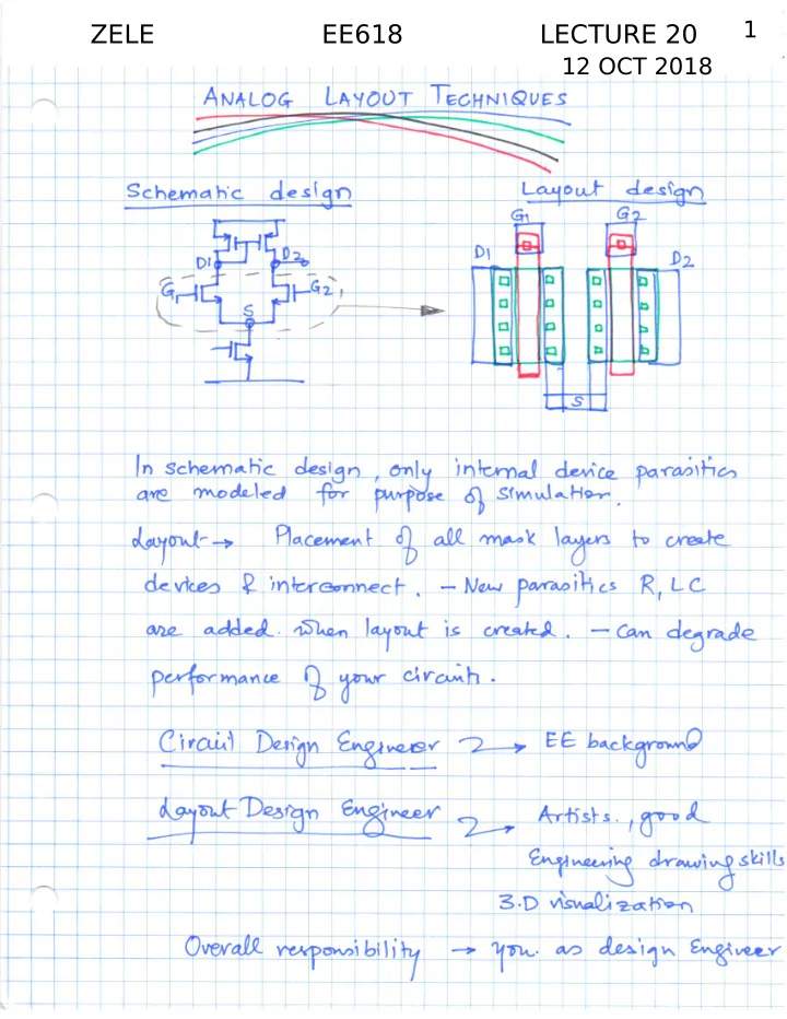
SLIDE 1
ZELE EE618 LECTURE 20
12 OCT 2018 1
SLIDE 2
ZELE EE618 L-20
2
SLIDE 3
ZELE EE618 L-20
3
SLIDE 4
ZELE EE618 L-20
4
SLIDE 5
ZELE EE618 L-20
5
SLIDE 6
ZELE EE618 L-20
6
SLIDE 7
ZELE EE618 L-20
7
SLIDE 8
ZELE EE618 L-20
8
SLIDE 9
ZELE EE618 L-20
9
SLIDE 10
ZELE EE618 L-20
10
SLIDE 11
ZELE EE618 L-20
11
SLIDE 12
ZELE EE618 L-20
12
SLIDE 13
ZELE EE618 L-20
13
SLIDE 14
ZELE EE618 L-20
14
SLIDE 15
ZELE EE618 L-20
15
SLIDE 16
ZELE EE618 L-20
16
SLIDE 17
ZELE EE618 L-20
17
SLIDE 18
Sample of Design Rules provided by the foundry
(Below shown rules doesn’t correspond to SCL process) MIM Capacitor Top plate connected to M6 M5 acts as botuom plate Dielectric thickness = 56nm
Interconnect layers (Doesn’t correspond to SCL process)
ZELE EE618 L-20
18
SLIDE 19
Basic Layers in SCL 180nm Difgerent ways of forming Diode Difgerent ways of forming BJT
ZELE EE618 L-20
19
SLIDE 20
Contacts to regions
Top View of NMOS Cross sectjonal view of NMOS Top View of PMOS Cross sectjonal view of PMOS
ZELE EE618 L-20
20
SLIDE 21
NMOS Total width = (0.5um) x 2 fjngers = 1um Length= 0.18 um NMOS Total width = (0.5um) x 2 multjples = 1um Length= 0.18 um
Difgusion resistors
ZELE EE618 L-20
21
SLIDE 22
Poly resistors
ZELE EE618 L-20
22
SLIDE 23
Mk-1 Mk MOM Capacitors
htups://web.stanford.edu/class/ee311/NOTES/Interconnect_Al.pdf
Electromigratjon failure
ZELE EE618 L-20
23
SLIDE 24
Layout of the Input Pair of OpAmp using Common-Centroid Comparator Schematjc Layout
ZELE EE618 L-20
24