LECTURE 3 1 ZELE EE618 6AUG2019 L-3 2 ZELE EE618 L-3 3 ZELE - - PDF document

LECTURE 3 1 ZELE EE618 6AUG2019 L-3 2 ZELE EE618 L-3 3 ZELE - - PDF document
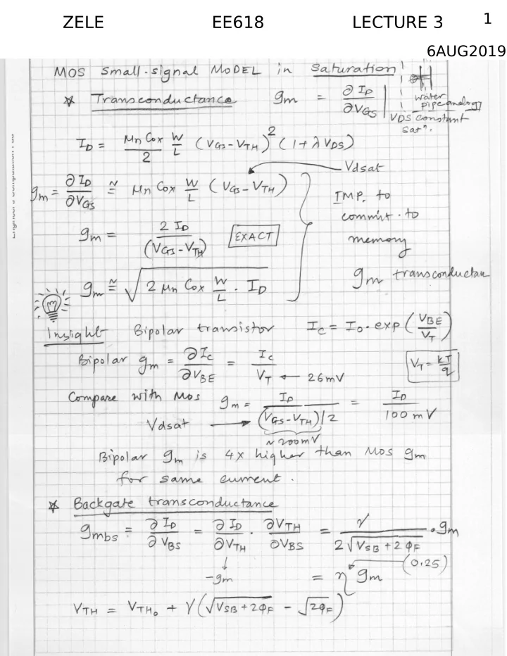
LECTURE 3 1 ZELE EE618 6AUG2019 L-3 2 ZELE EE618 L-3 3 ZELE EE618 L-3 4 ZELE EE618 L-3 5 ZELE EE618 L-3 6 ZELE EE618 L-3 7 ZELE EE618 EE618 (Zele) Body Effect and Sub-threshold Conduction Body Effect Consider the simplified
ZELE EE618 L-3
2
ZELE EE618 L-3
3
ZELE EE618 L-3
4
ZELE EE618 L-3
5
ZELE EE618 L-3
6
ZELE EE618 L-3
7
EE618 (Zele)
Body Effect and Sub-threshold Conduction
Body Effect
Consider the simplified NMOS shown in Fig. 1 part (A). A voltage VGS is applied between gate and source whereas a voltage VSB is applied between the source and bulk of the NMOS. For this explanation, we consider that the bulk is a p-well so that we can separately bias it (NMOS in a chip may lie in substrate and substrate of the whole chip will be tied to ground ). We consider the following two cases - CASE 1: VGS = VT H and VSB = 0 V As shown in Fig. 1 part (B), Due to positive VGS the holes in the channel region move out leaving negatively charged ions behind. The electrons that form the inversion layer comes from the n+(very high concentration) source region. The current in the device will be due to drift of these electrons when a VDS is applied. CASE 2: VGS = VT H and VSB >0 V In this case we are increasing VSB (can be achieved by decreasing the bulk voltage keeping source voltage constant). Due to a net positive voltage on the source as compared to the bulk, some of the electrons present in the channel will be attracted back in the source as shown in of Fig. 1 part (C). Hence to achieve the same charge density as in CASE1 we need a more positive charge on the gate. Therefore we can say that increasing VSB increases threshold voltage.
+ − + −
S D
VGS VSB
Bulk
n+ n+ p-well + −
S D
VGS
Bulk
n+ n+ p-well + − + −
S D
VGS VSB
Bulk
n+ n+ p-well
A B C
Figure 1: Body effect in MSOFETS
Effect of VDS in Subthreshold Region
- The region where VGS of the device is less than or close to VT H is known as sub-threshold region.
- Due to diffusion of minority charge carrier electrons, some leakage current may flow in the device even when VGS
is less than VT H.
- For a constant VDS, the current equation in subthereshold region is given as
Isubth = IO × exp( VGS
ζVT ) × (1 − exp( −VDS VT
)) where ζ is a non-ideality factor greater than 1 and VT = KT/q
- For VDS = 0, the current Isubth = 0.
- For VDS >4VT H or 5VT H the equation reduces to
Isubth = IO × exp( VGS
ζVT )
1