
SLIDE 1
Slides for Lecture 32
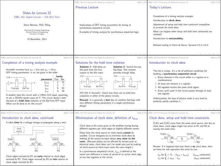
ENEL 353: Digital Circuits — Fall 2013 Term Steve Norman, PhD, PEng Electrical & Computer Engineering Schulich School of Engineering University of Calgary 25 November, 2013 ENEL 353 F13 Section 02 Slides for Lecture 32 slide 2/19Previous Lecture
Implications of DFF timing parameters for timing of synchronous sequential circuits. Examples of timing analysis for synchronous sequential logic. ENEL 353 F13 Section 02 Slides for Lecture 32 slide 3/19Today’s Lecture
Completion of a timing analysis example. Introduction to clock skew. Adjustment of setup and hold time constraint inequalities to account for clock skew. What can happen when setup and hold time constraints are violated? Introduction to metastability. Related reading in Harris & Harris: Sections 3.5.2–3.5.4 ENEL 353 F13 Section 02 Slides for Lecture 32 slide 4/19Completion of a timing analysis example
Available inverters have tcd = 9 ns and tpd = 15 ns. DFF timing parameters, in ns, are given in the table. FooLogic BarTron CLK Y family parameter Foo Bar tsetup 2 20 thold 1 7 tpcq 8 50 tccq 5 30 A student tests the circuit with a 1 MHz CLK input, expecting to see a 250 kHz square wave on Y. The circuit doesn’t work because of a hold time violation at the BarTron DFF input. What can be done to fix the circuit? ENEL 353 F13 Section 02 Slides for Lecture 32 slide 5/19Solutions for the hold time violation
Solution 1: Add delay on the path from the Foo- utput to the Bar input.
Introduction to clock skew
This list is review. It’s a list of sufficient conditions for building a synchronous sequential circuit . . .- 1. Every element in the circuit either is a register or is
- 2. At least one element is a register.
- 3. All registers receive the same clock signal.
- 4. Every cyclic path in the circuit passes through at least
- ne register.
Introduction to clock skew, continued
It takes time for a voltage change to propagate along a wire. clock source R1 Q1 D1 R2 Q2 D2 R3 Q3 D3 CLK1 CLK2 CLK3 Clock edges received by R1 are early relative to clock edges received by R2. Clock edges received by R3 are late relative to clock edges received by R2. ENEL 353 F13 Section 02 Slides for Lecture 32 slide 8/19Minimization of clock skew; definition of tskew
Clock skew is the name given to the problem having having different registers get clock edges at slightly different names. Delay from the clock source to clock inputs cannot be- avoided. Circuit designers try to minimize clock skew by
- same. (Because delays can be affected by factors such as
Clock skew, setup and hold time constraints
CLK1 and CLK2 come from the same clock source, but due to clock skew, clock edges might not arrive at R1 and R2 at exactly the same time. C L Q1 D1 Q2 D2 R1 R2 CLK1 CLK2 Review: If it happens that that there is no clock skew, then we know for safe operation this must be true . . . tpd for C L ≤ TC − (tpcq + tsetup) (tsetup constraint) tcd for C L ≥ thold − tccq (thold constraint)