Previous Lecture Todays Lecture Slides for Lecture 27 ENEL 353: - - PowerPoint PPT Presentation

previous lecture today s lecture slides for lecture 27
SMART_READER_LITE
LIVE PREVIEW

Previous Lecture Todays Lecture Slides for Lecture 27 ENEL 353: - - PowerPoint PPT Presentation

ENEL 353 F13 Section 02 Slides for Lecture 27 slide 2/19 ENEL 353 F13 Section 02 Slides for Lecture 27 slide 3/19 Previous Lecture Todays Lecture Slides for Lecture 27 ENEL 353: Digital Circuits Fall 2013 Term Review of the steps


slide-1
SLIDE 1

Slides for Lecture 27

ENEL 353: Digital Circuits — Fall 2013 Term Steve Norman, PhD, PEng Electrical & Computer Engineering Schulich School of Engineering University of Calgary 13 November, 2013 ENEL 353 F13 Section 02 Slides for Lecture 27 slide 2/19

Previous Lecture

Detailed discussion of an example from the textbook: the traffic light controller FSM. ENEL 353 F13 Section 02 Slides for Lecture 27 slide 3/19

Today’s Lecture

Review of the steps involved in designing a Moore FSM. A “divide-by-3 counter” FSM design problem, solved with binary state encoding, and solved again with “one-hot” encoding. Introduction to “sequence detection” problems, and solution using Moore and Mealy FSMs. Related reading in Harris & Harris: Sections 3.4.2, 3.4.3 ENEL 353 F13 Section 02 Slides for Lecture 27 slide 4/19

Moore FSM structure of traffic light controller (slide repeated from previous lecture)

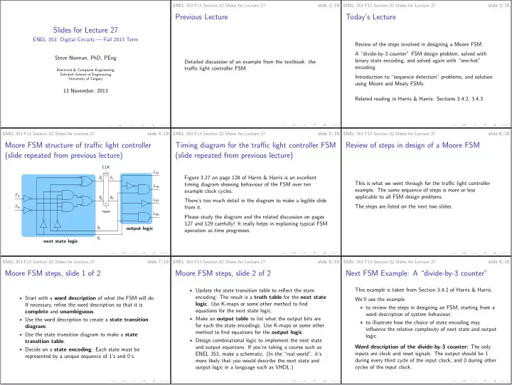
LA1 LB1 LB0 LA0 S′ 1 S1 reset TA TB S′ S0 CLK r S1 S0 next state logic
  • utput logic
ENEL 353 F13 Section 02 Slides for Lecture 27 slide 5/19

Timing diagram for the traffic light controller FSM (slide repeated from previous lecture)

Figure 3.27 on page 128 of Harris & Harris is an excellent timing diagram showing behaviour of the FSM over ten example clock cycles. There’s too much detail in the diagram to make a legible slide from it. Please study the diagram and the related discussion on pages 127 and 129 carefully! It really helps in explaining typical FSM
  • peration as time progresses.
ENEL 353 F13 Section 02 Slides for Lecture 27 slide 6/19

Review of steps in design of a Moore FSM

This is what we went through for the traffic light controller
  • example. The same sequence of steps is more or less
applicable to all FSM design problems. The steps are listed on the next two slides. ENEL 353 F13 Section 02 Slides for Lecture 27 slide 7/19

Moore FSM steps, slide 1 of 2

◮ Start with a word description of what the FSM will do. If necessary, refine the word description so that it is complete and unambiguous. ◮ Use the word description to create a state transition diagram. ◮ Use the state transition diagram to make a state transition table. ◮ Decide on a state encoding: Each state must be represented by a unique sequence of 1’s and 0’s. ENEL 353 F13 Section 02 Slides for Lecture 27 slide 8/19

Moore FSM steps, slide 2 of 2

◮ Update the state transition table to reflect the state
  • encoding. The result is a truth table for the next state
  • logic. Use K-maps or some other method to find
equations for the next state logic. ◮ Make an output table to list what the output bits are for each the state encodings. Use K-maps or some other method to find equations for the output logic. ◮ Design combinational logic to implement the next state and output equations. If you’re taking a course such as ENEL 353, make a schematic. (In the “real world”, it’s more likely that you would describe the next state and
  • utput logic in a language such as VHDL.)
ENEL 353 F13 Section 02 Slides for Lecture 27 slide 9/19

Next FSM Example: A “divide-by-3 counter”

This example is taken from Section 3.4.2 of Harris & Harris. We’ll use the example ◮ to review the steps in designing an FSM, starting from a word description of system behaviour; ◮ to illustrate how the choice of state encoding may influence the relative complexity of next state and output logic. Word description of the divide-by-3 counter: The only inputs are clock and reset signals. The output should be 1 during every third cycle of the input clock, and 0 during other cycles of the input clock.
slide-2
SLIDE 2 ENEL 353 F13 Section 02 Slides for Lecture 27 slide 10/19

Divide-by-3 counter: Waveforms and a state transition diagram

CLK Y (a) S0 Y: 1 S1 Y: 0 S2 Y: 0 Reset (b) Image is taken from Figure 3.28 from Harris D. M. and Harris S. L., Digital Design and Computer Architecture, 2nd ed., c 2013, Elsevier, Inc. ENEL 353 F13 Section 02 Slides for Lecture 27 slide 11/19

“A divide-by-N counter has one output and no inputs.”

The title of this slide is a quote from page 129 of Harris and Harris. Does it make sense to say there are no inputs? Every FSM needs a clock input. And the state transition diagram for the divide-by-3 counter also shows a reset input. Important: In discussion of FSMs, it’s traditional to count the number of inputs as the number of system input signals used by the next state logic. For whatever reason, important input signals—such as CLK and reset—that go straight to the state register do not count in the number of FSM inputs. ENEL 353 F13 Section 02 Slides for Lecture 27 slide 12/19

Divide-by-3 counter with binary state encoding

Let’s finish the design of the counter using unsigned binary encoding for the states S0, S1, and S2. Unlike what is done in the textbook, we’ll put the unused state 11 into our truth tables with the goal of using don’t-care
  • utputs to simplify the next-state and output equations.
ENEL 353 F13 Section 02 Slides for Lecture 27 slide 13/19

Divide-by-3 counter with one-hot encoding

One-hot state encoding requires one flip-flop for each state. In any state, a single state bit is TRUE and all the others are FALSE. One-hot state encodings for a system with three states: 001, 010, 100. One-hot state encodings for a system with four states: 0001, 0010, 0100, 1000. Let’s complete the divide-by-3 FSM design using one-hot state encoding, then make a few remarks. We’ll assume that we can build a state register out of resettable DFFs and/or settable DFFs, whatever is needed to make the reset logic work. ENEL 353 F13 Section 02 Slides for Lecture 27 slide 14/19

Sequence detection problems

Most textbooks on digital design present several FSM design problems that are worded something like this example: “Design an FSM that will have an output of 1 only when the input is 0, but was 1 for the previous three clock cycles.” Example 3.7 from Harris & Harris: “Alyssa P. Hacker owns a pet robotic snail with an FSM brain. The snail crawls from left to right along a paper tape containing a sequence of 1’s and 0’s. On each clock cycle, the snail crawls to the next bit. The snail smiles when the last two bits it has crawled over are, from left to right, 01. Design the FSM [. . . ]” Problems of this kind are great practice for students, because solving them requires careful thought about states and state transitions. ENEL 353 F13 Section 02 Slides for Lecture 27 slide 15/19

Useful assumptions for sequence detection problems

First, let’s assume that the clock period is long compared to switching times for the available circuit elements. That way, we can ignore timing problems caused by excessive delays in circuit elements. Second, let’s assume that the input will be “reasonable”, in the following senses: ◮ The input makes at most one 0 → 1 or 1 → 0 transition within any single clock cycle. ◮ The input never makes a 0 → 1 or 1 → 0 transition really near in time to a rising clock edge. (This eliminates uncertainty about DFF D input values when those values are being copied to DFF Q outputs.) ENEL 353 F13 Section 02 Slides for Lecture 27 slide 16/19

Which of A, B, C and D are “reasonable” inputs for sequence detection?

CLK 1 A 1 1 1 1 t0 t1 t2 t3 t4 B C D ENEL 353 F13 Section 02 Slides for Lecture 27 slide 17/19

Review: Moore and Mealy FSM structures

Which is which? How can you tell? (a)
  • utput
logic next state logic state next state k k M N inputs
  • utputs
CLK (b) next state logic
  • utput
logic N
  • utputs
state next state k k inputs M CLK ENEL 353 F13 Section 02 Slides for Lecture 27 slide 18/19

A sequence detection problem

Problem statement: Design an FSM to detect the following sequence of bits on the FSM input: 1 for three clock cycles followed by a 0. The output should be 1 when the sequence has been detected and 0 at other times. We’ll consider both Moore and Mealy FSM designs. For each of the Moore and Mealy designs, what does the problem statement mean, in terms of the current input value and the values of the input at recent clock edges? Let’s make a timing diagram to be really clear about how the Moore and Mealy outputs will react to a typical input signal.
slide-3
SLIDE 3 ENEL 353 F13 Section 02 Slides for Lecture 27 slide 19/19

Upcoming topics

Moore and Mealy state transition diagrams for the sequence detection problem. Completion of next state and output logic design for the Mealy FSM. Factoring of FSMs. Reverse-engineering an FSM: Given a circuit, find a word description of what the FSM does. Related reading in Harris & Harris: Sections 3.4.3–3.4.6