Previous Lecture Todays Lecture Slides for Lecture 12 ENEL 353: - - PowerPoint PPT Presentation

previous lecture today s lecture slides for lecture 12
SMART_READER_LITE
LIVE PREVIEW

Previous Lecture Todays Lecture Slides for Lecture 12 ENEL 353: - - PowerPoint PPT Presentation

ENEL 353 F13 Section 02 Slides for Lecture 12 slide 2/19 ENEL 353 F13 Section 02 Slides for Lecture 12 slide 3/19 Previous Lecture Todays Lecture Slides for Lecture 12 ENEL 353: Digital Circuits Fall 2013 Term A little more about


slide-1
SLIDE 1

Slides for Lecture 12

ENEL 353: Digital Circuits — Fall 2013 Term Steve Norman, PhD, PEng Electrical & Computer Engineering Schulich School of Engineering University of Calgary 4 October, 2013 ENEL 353 F13 Section 02 Slides for Lecture 12 slide 2/19

Previous Lecture

Theorems T11, T11′, T12, T12′. Discussion of T12 and T12′: De Morgan’s Theorem. Using theorems to simplify equations. Going from logic equations to circuit designs. ENEL 353 F13 Section 02 Slides for Lecture 12 slide 3/19

Today’s Lecture

A little more about drawing schematics. (Related reading in Harris & Harris: Sections 2.4.) The concept of a minimal SOP expression. (Related reading: Section 2.3.5.) Multilevel combinational logic. (Related reading: Section 2.5.) We’ll just get started on unknown/illegal (X) and floating/high-impedance (Z) values in combinational logic. (Related reading: Section 2.6.) ENEL 353 F13 Section 02 Slides for Lecture 12 slide 4/19

Schematics: Guidelines for directions of information flow through circuit elements

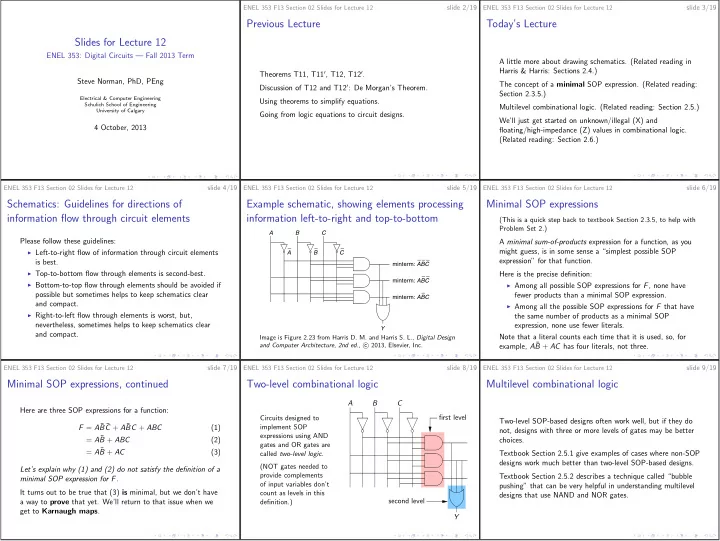
Please follow these guidelines: ◮ Left-to-right flow of information through circuit elements is best. ◮ Top-to-bottom flow through elements is second-best. ◮ Bottom-to-top flow through elements should be avoided if possible but sometimes helps to keep schematics clear and compact. ◮ Right-to-left flow through elements is worst, but, nevertheless, sometimes helps to keep schematics clear and compact. ENEL 353 F13 Section 02 Slides for Lecture 12 slide 5/19

Example schematic, showing elements processing information left-to-right and top-to-bottom

B A C Y minterm: ABC minterm: ABC minterm: ABC A B C Image is Figure 2.23 from Harris D. M. and Harris S. L., Digital Design and Computer Architecture, 2nd ed., c 2013, Elsevier, Inc. ENEL 353 F13 Section 02 Slides for Lecture 12 slide 6/19

Minimal SOP expressions

(This is a quick step back to textbook Section 2.3.5, to help with Problem Set 2.) A minimal sum-of-products expression for a function, as you might guess, is in some sense a “simplest possible SOP expression” for that function. Here is the precise definition: ◮ Among all possible SOP expressions for F, none have fewer products than a minimal SOP expression. ◮ Among all the possible SOP expressions for F that have the same number of products as a minimal SOP expression, none use fewer literals. Note that a literal counts each time that it is used, so, for example, A¯ B + AC has four literals, not three. ENEL 353 F13 Section 02 Slides for Lecture 12 slide 7/19

Minimal SOP expressions, continued

Here are three SOP expressions for a function: F = A¯ B ¯ C + A¯ BC + ABC (1) = A¯ B + ABC (2) = A¯ B + AC (3) Let’s explain why (1) and (2) do not satisfy the definition of a minimal SOP expression for F. It turns out to be true that (3) is minimal, but we don’t have a way to prove that yet. We’ll return to that issue when we get to Karnaugh maps. ENEL 353 F13 Section 02 Slides for Lecture 12 slide 8/19

Two-level combinational logic

Circuits designed to implement SOP expressions using AND gates and OR gates are called two-level logic. (NOT gates needed to provide complements
  • f input variables don’t
count as levels in this definition.) second level first level A B C Y ENEL 353 F13 Section 02 Slides for Lecture 12 slide 9/19

Multilevel combinational logic

Two-level SOP-based designs often work well, but if they do not, designs with three or more levels of gates may be better choices. Textbook Section 2.5.1 give examples of cases where non-SOP designs work much better than two-level SOP-based designs. Textbook Section 2.5.2 describes a technique called “bubble pushing” that can be very helpful in understanding multilevel designs that use NAND and NOR gates.
slide-2
SLIDE 2 ENEL 353 F13 Section 02 Slides for Lecture 12 slide 10/19

Hardware reduction via multilevel design

Textbook reference: Section 2.5.1. Definition of N-input XOR: XOR(A1, A2, . . . , AN) = 1 if the number of 1 inputs is odd if the number of 1 inputs is even Page 70 in the textbook shows that the 3-input XOR (which happens to be the sum function of a 1-bit full adder) requires four 3-input AND gates and a 4-input OR gate to implement the minimal SOP expression. The textbook goes on to show that 3-input XOR can be implemented using only two 2-input XOR gates—a significant improvement over the SOP-based circuit. ENEL 353 F13 Section 02 Slides for Lecture 12 slide 11/19

Hardware reduction via multilevel design, continued

Textbook reference: Section 2.5.1. Continuing to follow the textbook presentation, consider the problem of implementing an 8-input XOR function. Below are two choices. (Of course there are other choices as well.) Two-level, SOP-based: ◮ 128 8-input AND gates! ◮ One 128-input OR gate! Three-level “tree” of seven 2-input XOR gates: ENEL 353 F13 Section 02 Slides for Lecture 12 slide 12/19

Alternative interpretations of NAND and NOR

Remember that De Morgan’s Theorem says things such as ABC = ¯ A + ¯ B + ¯ C and A + B + C + D = ¯ A¯ B ¯ C ¯ D. That results in alternate symbols for NAND and NOR gates, for example: . . . can be thought of as . . . . . . can be thought of as . . . You can think of moving bubbles through gates and interchanging AND with OR as bubble pushing. Bubble pushing does not change the behaviour of a gate. ENEL 353 F13 Section 02 Slides for Lecture 12 slide 13/19

Bubble pushing for analysis of circuits with NAND and NOR gates

Textbook reference: Section 2.5.2. This is a procedure to allow interpretation of logic in terms of ORs and ANDs rather than NANDs and NORs . . . ◮ Start at the output and work towards the inputs. ◮ If the gate that drives the overall output is NAND or NOR, push its bubble to its inputs. ◮ For all the other gates, push bubbles as necessary so that each internal wire has either no bubbles or cancelling bubbles at both ends. ENEL 353 F13 Section 02 Slides for Lecture 12 slide 14/19

Bubble pushing for analysis of circuits with NAND and NOR gates—example

Y A B C D Let’s use bubble pushing to express Y in terms of AND and OR operations, perhaps with NOT applied to some of the inputs.

There is a similar example starting near the bottom of page 71 in the textbook. ENEL 353 F13 Section 02 Slides for Lecture 12 slide 15/19

Illegal (X) and Floating (Z) Values in Logic Circuits

Textbook reference: Section 2.6. In pure Boolean algebra, a variable can have only one of two values: 0 or 1. However, in modeling logic circuits, it’s sometimes useful to have a more complex model. This model says that a node in a circuit can have one of four values: 0, 1, X or Z. Before getting into the details of what X and Z values mean, it’s helpful to understand a very approximate model of how logic gates work . . . ENEL 353 F13 Section 02 Slides for Lecture 12 slide 16/19

Basic structure of a CMOS logic gate

The pull-up and pull-down networks are collections of MOS
  • transistors. (Details of MOS transistors are a major topic in
courses later in the ENEL degree program.) pull-up network pull-down network inputs GND
  • utput
VDD SMALL resistance when output should be 1 SMALL resistance when output should be 0 In normal operation one of the pull-up/pull-down networks is ON and the other one is OFF. Which network is ON and which is OFF depends on the bit pattern on the input wires. ENEL 353 F13 Section 02 Slides for Lecture 12 slide 17/19

Simple model for a CMOS gate with LOW output

This should give you an idea why the voltage on the output is near 0 V . . . pull-up network is OFF . . . near INFINITE resistance pull-down network is ON . . . SMALL resistance GND
  • utput
VDD inputs The actual behaviour of the transistors inside the pull-up and pull-down networks is more complicated than this model suggests! ENEL 353 F13 Section 02 Slides for Lecture 12 slide 18/19

Simple model for a CMOS gate with HIGH output

This should give you an idea why the voltage on the output is near VDD . . . pull-up network is ON . . . SMALL resistance pull-down network is OFF . . . near INFINITE resistance GND
  • utput
VDD inputs Again, real circuit behaviour is not quite this simple.
slide-3
SLIDE 3 ENEL 353 F13 Section 02 Slides for Lecture 12 slide 19/19

Upcoming topics

Completion of material on X and Z values at nodes of logic circuits. Karnaugh maps (also known as K-maps). Related reading in Harris & Harris: Sections 2.6 and 2.7