
SLIDE 1
Advanced VLSI Design CMOS Inverter I CMPE 640 1 (11/8/04)
UMBC
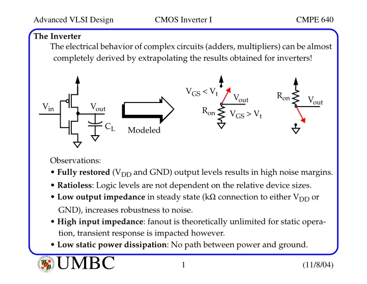
U M B C U N I V E R S I T Y O F M A R Y L A N D B A L T I M O R E C O U N T Y 1 9 6 6The Inverter The electrical behavior of complex circuits (adders, multipliers) can be almost completely derived by extrapolating the results obtained for inverters! Observations:
- Fully restored (VDD and GND) output levels results in high noise margins.
- Ratioless: Logic levels are not dependent on the relative device sizes.
- Low output impedance in steady state (kΩ connection to either VDD or
GND), increases robustness to noise.
- High input impedance: fanout is theoretically unlimited for static opera-
tion, transient response is impacted however.
- Low static power dissipation: No path between power and ground.
Vout Vin CL Modeled Ron Vout Ron Vout VGS < Vt VGS > Vt