
SLIDE 1
The transistor – a switch with no moving parts
William Sandqvist william@kth.se
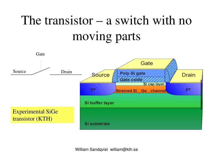
Experimental SiGe transistor (KTH)
Source Drain Gate
The transistor a switch with no moving parts Gate Source Drain - - PowerPoint PPT Presentation
The transistor a switch with no moving parts Gate Source Drain Experimental SiGe transistor (KTH) William Sandqvist william@kth.se Why CMOS? CMOS-Transistors are easy to manifacture CMOS-Transistors are made of ordinary sand
William Sandqvist william@kth.se
Experimental SiGe transistor (KTH)
Source Drain Gate
William Sandqvist william@kth.se
William Sandqvist william@kth.se
”Pull Up” ”Pull Down”
William Sandqvist william@kth.se
William Sandqvist william@kth.se
(a) Circuit V
f
V
DD
V
x
(b) Truth table and transistor states
1 1 f x T
1
T
2
T
1 T 2
A CMOS-circuit consists of both PMOS and NMOS circuits. The acronym CMOS stands for (Complementary MOS).
William Sandqvist william@kth.se
V
f
V
DD
V
x
T
1
T
2
William Sandqvist william@kth.se
VLmin VILmax VIHmin VHmax VOHmin VOLmax Margins!
William Sandqvist william@kth.se
Vin V
Unstable point
VDD VDD
transfer function
unstable point, when both T1 and T2 is conducting.
mode, it enters a state called metastability.
then the transistors in the circuit can be damaged by the high current.
William Sandqvist william@kth.se
DD C F DD C F 2
”1” ”0” ”1”→ ”0” ”1”← ”0”
C C
William Sandqvist william@kth.se
VDD VOH VSS VA VB VA VB VOH VSS(0) VSS(0) VDD(1) VSS(0) VDD(1) VDD(1) VDD(1) VSS(0) VDD(1) VDD(1) VDD(1) VSS(0)
William Sandqvist william@kth.se
VDD VOH VSS VA VB VA VB VOH VSS(0) VSS(0) VDD(1) VSS(0) VDD(1) VSS(0) VDD(1) VSS(0) VSS(0) VDD(1) VDD(1) VSS(0)
William Sandqvist william@kth.se
William Sandqvist william@kth.se
William Sandqvist william@kth.se
William Sandqvist william@kth.se
A Q E E
TG= 2 Transistors
A Q E
V
A
VE VOH L L Z L H L H L Z H H H
A Q E E E
William Sandqvist william@kth.se
William Sandqvist william@kth.se
X Y Q S
Q=XS+YS
William Sandqvist william@kth.se
X Y Q S X Y Q S
Q=XS+YS
William Sandqvist william@kth.se
2 MOS 2 MOS 2 MOS
William Sandqvist william@kth.se
2 MOS 2 MOS 2 MOS 2 MOS
William Sandqvist william@kth.se
William Sandqvist william@kth.se
William Sandqvist william@kth.se
William Sandqvist william@kth.se
William Sandqvist william@kth.se
Area: AMUX= 2+6+6+6=20 Transistors Delay: TMUX= 5TNAND Area: AMUX=2+4+4 = = 10 Transistors Delay: TMUX= 3TNAND DeMorgan Area: AMUX= 6 Transistors Delay: TMUX= ~2TNAND NAND-NAND AND-OR
William Sandqvist william@kth.se
Area: AXOR=2+2+6+6+6=22 Transistors Delay: TXOR=5TNAND Area: AXOR=2+2+4+4=12 Transistors Delay: TXOR=3TNAND DeMorgan Area: AXOR=8 Transistorer Delay: TXOR=~2TNAND Area: AXOR=4+4+4+4=16 Transistors Delay: TXOR=3TNAND Nand only
William Sandqvist william@kth.se
William Sandqvist william@kth.se
VA VB VC VQ
3-input NAND
VDD VSS
William Sandqvist william@kth.se
DeMorgan
William Sandqvist william@kth.se
William Sandqvist william@kth.se
(b) Equivalent circuit for timing purposes
x f (a) Inverter that drives n
To inputs of n
To inputs of n
x V
f
N
1
Cn= n⋅C
William Sandqvist william@kth.se
for n = 1 V
f
for n = 4 V
f
V
DD
Gnd Time
William Sandqvist william@kth.se
William Sandqvist william@kth.se
Non-inverting Buffer Tri-state Buffer High-Fan-Out Buffer
W 3W
En x f f x En x En f Z 1 1 Z 1 1 1
William Sandqvist william@kth.se
x0 x1 x2
2 1 2 2 1
William Sandqvist william@kth.se
x0 x1 x2
2 1 2 2 1
William Sandqvist william@kth.se
William Sandqvist william@kth.se
x1 x2 f Two-input LUT
Programmable cells
1 1 1
A LUT with n inputs can realize all combinational functions with n inputs The usual size in an FPGA is n=4
x1 x2 f Two-input LUT
Programmed values
1 1 1
Multiplexer
William Sandqvist william@kth.se
2 1
William Sandqvist william@kth.se
William Sandqvist william@kth.se
William Sandqvist william@kth.se
V
DD x
1
x
2
x
3
f
7404 7408 7432
3 2 2 1
William Sandqvist william@kth.se
3 2 2 1
William Sandqvist william@kth.se
William Sandqvist william@kth.se
3 2 1 3 2 1 3 2 1 3 2 1
William Sandqvist william@kth.se
William Sandqvist william@kth.se
1:1
1:2 2:1
1:3 1:4 2:2 2:13 2:12 1:13 1:12 2:10 2:11 2:9 2:8 3:1 3:13 3:2 3:3 3:4 3:5 3:12 3:6 4:1 4:2 4:4 4:5 4:6
William Sandqvist william@kth.se
William Sandqvist william@kth.se
William Sandqvist william@kth.se
William Sandqvist william@kth.se
William Sandqvist william@kth.se