
SLIDE 1
1
MOS Transistor
Professor Chris H. Kim
University of Minnesota
- Dept. of ECE
chriskim@umn.edu www.umn.edu/~chriskim/
2
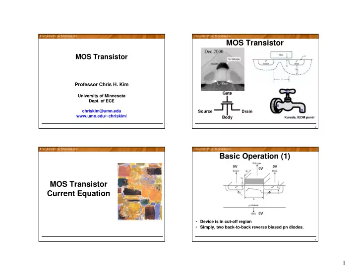
MOS Transistor
Drain Source Gate
Kuroda, IEDM panel
Body
MOS Transistor Current Equation
4
Basic Operation (1)
- Device is in cut-off region
- Simply, two back-to-back reverse biased pn diodes.