
SLIDE 1
Principles of VLSI Design Details of the MOS Transistor CMSC 491B/711 1 (December 4, 2000 6:10 pm)
UMBC
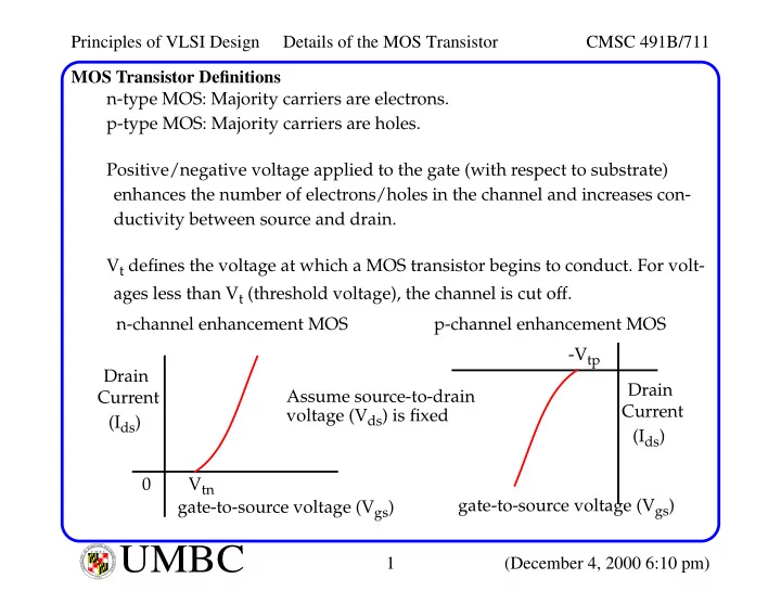
U M B C U N I V E R S I T Y O F M A R Y L A N D B A L T I M O R E C O U N T Y 1 9 6 6MOS Transistor Definitions n-type MOS: Majority carriers are electrons. p-type MOS: Majority carriers are holes. Positive/negative voltage applied to the gate (with respect to substrate) enhances the number of electrons/holes in the channel and increases con- ductivity between source and drain. Vt defines the voltage at which a MOS transistor begins to conduct. For volt- ages less than Vt (threshold voltage), the channel is cut off. gate-to-source voltage (Vgs) Drain (Ids) Current Vtn n-channel enhancement MOS
- Vtp
Drain (Ids) Current p-channel enhancement MOS gate-to-source voltage (Vgs) Assume source-to-drain voltage (Vds) is fixed