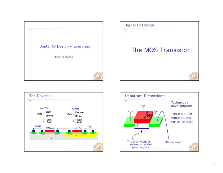
The MOS Transistor Johan Lfgren The Devices Important Dimensions - - PowerPoint PPT Presentation

the mos transistor
SMART_READER_LITE
LIVE PREVIEW

The MOS Transistor Johan Lfgren The Devices Important Dimensions - - PowerPoint PPT Presentation

Digital IC Design Digital IC Design Exercises The MOS Transistor Johan Lfgren The Devices Important Dimensions Technology development: Gate NMOS PMOS Drain Source Source Drain Drain Source S Gate 1993: 0.6 um Gate W


slide-1
SLIDE 1

1

Digital IC Design – Exercises

Johan Löfgren

Digital IC Design

The MOS Transistor

The Devices

Drain

NMOS

S

PMOS VDD GND NMOS PMOS

With Bulk Drain Source Gate With Bulk Drain Source Gate

G S D G S D 3 p- n+ n+ p+ p+ n- p+ n+ S D S D

Important Dimensions

Gate Source Drain

Technology development:

tox

L W

Source

1993: 0.6 um 2003: 65 nm 2013: 18 nm?

4

L

The technology is named after the gate length L “Diode area”

slide-2
SLIDE 2

2

VGS=5V Linear Region

I D as a function of VDS

Slope due to

Resistive

  • peration

ID VGS=3V VGS=4V g Saturation VDS = VGS-VT

channel length modulation

5 1 2 3 4 5 VDS [V] VGS 3V

MOS Model for Long Channels

Widely used model for manual calculations

2 2

´

  • ;

(

  • ) (1

) 2

  • ;

´ ((

  • )
  • )(1

) 2 λ λ ≥ = + < = +

n DS GS T D GS T DS DS DS GS T D n GS T DS DS

k W V V V I V V V L V W V V V I k V V V V L

6

´ (

  • 2
  • 2

) μ γ φ φ = = + +

SB

n n

  • x

T T F F

k C V V V Often added to avoid discontinuity

Problem 1

Given the data in the table for an NMOS transistor with k´=20μA/V2, l l t V λ d W/L

VGS(V) VDS(V) VSB(V) ID(μA) 1 3 5 1210 2 5 5 4410 3 5 10 5292

calculate VT0, λ, and W/L.

7

Velocity Saturation

VDS forms a horizontal E-field An increased E-field leads to higher electron velocity However at a critical E field the velocity saturates due

( )

sat

υ

( ) ξ ( ) ξ

However at a critical E-field , the velocity saturates due to collisions with other atoms

Drain Source

5 m

10 for both electrons and holes s

sat

υ ≈

( )

c

ξ

8

p- n+ n+

Drain VDS establish a horizontal E-field Source

slide-3
SLIDE 3

3

I D versus VDS Long-channel ID (mA)

0.5

VGS-VT = 2.5 - 0.43 = 2.07 V

Long channel device Short-channel device

0.4 0.3 0.2

VGS = VDD = 2.5 For both

9

2.5 0.5 2.0 1.5 1.0 0.1

VDS (V)

VDSAT = 0.63 V

A first order model for the velocity

Model for Manual Analysis

y saturated region:

2

(( ) ) 2

DSAT DSAT n

  • x

GS T DSAT

V W I C V V V L μ = − −

10

I D versus VDS

0 25 0 6

VDS = VGS - VT

Quadratic ID(VGS) Linear ID(VGS) 0 05 0.1 0.15 0.2 0.25 0.2 0.3 0.4 0.5 0.6 ID (mA) VGS= 2.5 VGS= 2.0 VGS= 1.5 VGS= 2.5 VGS= 2.0 VGS= 1.5 VGS= 1.0 ID (mA)

11

0.5 1 1.5 2 2.5 0.05 0.5 1 1.5 2 2.5 0.1 VDS (V) VGS= 1.0 Long Channel Short Channel

GS

VDS (V)

Conclusions - Static Behavior

2

´ (( ) ) 2

DS D n GS T DS

V W I k V V V L = − −

Linear Region VDS< VGS-VT

Long channel device

2

2 ´ ( ) (1 ) 2

n D GS T DS

L k W I V V V L λ = − +

DS GS T

Saturated Region VDS> VGS-VT

12

( 2 2 )

T T F SB F

V V V γ φ φ = + − + − −

Threshold Voltage

slide-4
SLIDE 4

4

Conclusions - Static Behavior

2 '

(( ) )(1 ) 2 Resistive

DS D n GS T DS DS

V W I k V V V V L λ = − − +

Short channel device

' 2

2 ( ) (1 ) Saturated 2

n D GS T DS

L k W I V V V L λ = − +

13

2 '

Ve (( locity saturated ) )(1 ) 2

DSAT D n GS T DSAT DS

V W I k V V V V L λ = − − +

Three Regions

VDSAT

0 15

(mA) I 2 V

GS

V = Linear Velocity saturated VDSAT= VGS-VT 1.06V

0.1 0.15

(mA)

D

I

GS

1.5 V

GS

V =

14

Saturated 0.63= VGS-0.43 VGS-VT

(V)

DS

V 0.5 1 2 1 V

GS

V =

A Unified Model for Manual Analysis

2 ' min min

(( ) )(1 ) 2 min( )

D n GS T DS

W I k V V V L V V V V V V V λ = − − + = −

15

min

min( , , )

GS T DS DSAT

V V V V V =

Problem 3a

250 50 100 150 200 Id [uA]

16

0,5 1 1,5 2 2,5 3 Vds [V] Vgs = 1 Vgs = 1,75 Vgs = 2,5 Saturation Voltage

slide-5
SLIDE 5

5

A PMOS Transistor

Velocity saturation is less pronounced for PMOS due to lower mobility

I ( A)

  • 0.04
  • 0.02

Assume all variables negative!

VGS = -1.0V VGS = -1.5V V = -2 0V ID (mA)

17

  • 2.5
  • 2
  • 1.5
  • 1
  • 0.5
  • 0.1
  • 0.08
  • 0.06

negative!

VGS = -2.0V VGS = -2.5V VDS (V)

Transistor Model for Manual Analysis

18

MOS Dynamic Behavior

Equivalent switching resistance V V VGS ≥ VT R

  • n

S D

ID VGS = VDD R0 Rmid ID VGS = VDD R0 Rmid

19

VDS VDD/2 VDD VDS VDD/2 VDD

Drain Source Gate

CGD CGS tox

MOS Capacitances

CDB

n+ n+

CG CSB

Bulk Cap. Junction Cap.

20

Xd

Overlap Cap.

slide-6
SLIDE 6

6

Junction Capacitance

CDiff = CBot + CSW Drain/ Source Diffusion

Bottom

CDiff CBot CSW

Don’t count the wall towards the channel

T

  • w

a r d s a n n e l

Bottom

G a t e 21 T C h a n

Side Wall

W Ls

Channel Capacitance

(Table 3-4) To Bulk To Source To Drain Total Gate Cap.

CGCB CGCS CGCD CG Cut off: No channel ⇒ CGC = CGCB

Cutoff COX W L COX W L + 2 C0W Resistive (1/2) COX W L (1/2) COX W L COX W L + 2 C0W Saturation (2/3) COX W L (2/3) COX W L + 2 C0W

22

Resistive: Channel ⇒ Divide CGC in two parts Saturation: ≈ 2/ 3 of Channel to source

Problem 8

BL2 BL1 GND

0.2x0.2 um

RWL

Cell Border Contact X

Tr Ts Tw

Node Y 23

WWL Calculate the capacitance in node Y if it consists of the gate capacitance in Ts and the drain capacitance in Tw. Cox = 5 fF/um2, Cj0 = 1.5 fF/um2, and Cjsw0 = 0.25 fF/m