Review EEE118: Electronic Devices and Circuits Introduced the idea - - PDF document

review eee118 electronic devices and circuits
SMART_READER_LITE
LIVE PREVIEW

Review EEE118: Electronic Devices and Circuits Introduced the idea - - PDF document

EEE118: Lecture 11 Review Review EEE118: Electronic Devices and Circuits Introduced the idea of a dynamic resistance or small signal Lecture XI resistance. Compared the voltage source model and th evenin model of a James E Green diode.


slide-1
SLIDE 1

EEE118: Electronic Devices and Circuits

Lecture XI James E Green

Department of Electronic Engineering University of Sheffield j.e.green@sheffield.ac.uk

1/ 22 2/ 22 EEE118: Lecture 11 Review

Review

Introduced the idea of a dynamic resistance or small signal resistance. Compared the voltage source model and th´ evenin model of a diode. Considered how capacitors can be used to block quiescent conditions (DC) but pass signals (AC). Introduced the idea of a small signal equivalent circuit - How the signal “sees” the circuit. Introduced the bipolar transistor. Briefly discussed two numbering systems for active devices.

3/ 22 EEE118: Lecture 11 Review

Outline

1 Review 2 BJT Modes of Operation 3 Characteristics

Input Characteristics Output Characteristics Transfer, Mutual or Transconductance (gm) Characteristics

4 Large Signal Model of a BJT 5 ZTX653 Large Signal Parameters 6 Large Signal Model of a MOSFET 7 IFR510 Characteristics 8 Switches 9 Switch Types

Mechanical Switches Electro-Mechanical Switches

10 Review 11 Bear

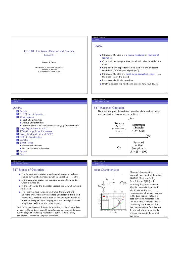
4/ 22 EEE118: Lecture 11 BJT Modes of Operation

BJT Modes of Operation

There are four possible modes of operation where each of the two junctions is either forward or reverse biased.

Forward Active (Amplifier) β ≈ 25 − 1000 Reverse Active

(in backwards...)

β ≈ 1 Saturation (Switch) “On” State Off VCB VBE

5/ 22 EEE118: Lecture 11 BJT Modes of Operation

BJT Modes of Operation II

The forward active region provides amplification of voltage and/or current (both means power amplification (P = IV )). In the saturation region the transistor appears like a switch which is turned on. In the ‘off’ region the transistor appears like a switch which is turned off. The reverse active region is used when the BE and CB junctions are accidentally exchanged (transistor in the circuit backwards). Performance is poor c.f forward active region as transistor designers adjust doping densities and region widths to optimise performance in other regions.

Note: some transistors are designed for amplification (linear) use others are designed for switching use. All transistors can perform both functions but the design of “switching” transistors is optimised for switching

  • applications. Likewise for “amplifier transistors”.

6/ 22 EEE118: Lecture 11 Characteristics Input Characteristics

Input Characteristics

− +

VBE IB

− +

VCE VBE

2 4 6 8 10 550 600 650 700 750 800 850 900 VBE [mV] IB [mA] Increasing VCE

1 V 34 V 67 V 100 V

Shape of characteristics essentially governed by the diode equation when VCE ≈ 0. IB = IS

  • exp
  • q VBE

k T

  • − 1
  • Increasing VCE with constant

VBE decreases the base width, slightly decreasing the recombination of minority carriers in the base region. Note, the base current is incidental, it is the base emitter voltage that is controlling the transistor. But like the compressor from Lecture 9, VBE will rise to whatever is necessary to admit the desired current IB

slide-2
SLIDE 2

7/ 22 EEE118: Lecture 11 Characteristics Output Characteristics

Output Characteristics

− +

VBE

− +

VCE IC

20 40 60 80 100 120 140 0.2 0.4 0.6 0.8 1.0 1.2 1.4 VCE [V] IC [mA] Increasing VBE

575 mV 625 mV 650 mV 662.5 mV 675 mV 686.5 mV 693 mV 700 mV

A family of curves showing effect

  • n the output VCE and IC as a

function of the input VBE (or IB). When VCE is small the transistor is in saturation both BE and CB junctions forward biased (transistor switched “on”) (left of graph). While VBE is too small to cause IC to rise above the leakage current level, the transistor is off (y ≈ 0 on the graph). Forward active region is indicated by nearly parallel characteristics.

8/ 22 EEE118: Lecture 11 Characteristics Transfer, Mutual or Transconductance (gm) Characteristics

Transfer Characteristics

− +

VBE

− +

VCE IC

20 40 60 80 100 120 140 160 575 600 625 650 675 700 VBE [V] IC [mA] Increasing VCE

1 V 34 V 67 V 100 V

The transfer characteristic relates the controlling voltage (VBE) to the controlled parameter IC. VBE is related to IC for a BJT by IC = IS

  • exp
  • q VBE

k T

  • − 1
  • and

by square law expressions for FETs (see handouts). This expression holds over many

  • rders of magnitude while the

relationship between base current and collector current changes considerably (hFE not constant). See Horowitz and Hill, second

  • Ed. pp 79 - 81 section 2.10 for

full details.

9/ 22 EEE118: Lecture 11 Large Signal Model of a BJT

Large signal BJT model

Large signals deal with active devices moving through large non-linear regions of their characteristics. A suitable large signal model for the forward active region of a BJT is to replace the base emitter junction with a 0.7 V source (it is a diode after all...) and to replace the reverse biased collector base junction with a current source where the current is controlled by the base current (the two are linked by the large signal current gain hFE 1) IC = hFE IB.2

− +

IB 0.7 V B E IC = hFEIB IC ≈ βFIB C

1note capital F and capital E means large signal parameters 2hFE hybrid model Forward, Emitter common. Also “Ebers-Moll transistor

model”, Millman and Grabel second ed. pp. 87 - 114.

10/ 22 EEE118: Lecture 11 Large Signal Model of a BJT

VBE is the controlling variable and IC is the controlled variable and IB is incidental (MOSFETs have no equivalent, IG). However, in the large signal model VBE is fixed at 0.7 V. How can it be the controlling variable if it is fixed? In switching applications we want the transistor to change from conducting to non-conducting (and back) as quickly as

  • possible. The load (whatever the collector is connected to)

defines the maximum value of IC. The designer ensures that the input to the transistor (whatever the base is connected to) is able to supply whatever base current (IB) is required to cause the transistor to switch. This makes the exact value of VBE and IB less important. In this way the dependence of the circuit operation on hFE is

  • lessened. This is desirable because hFE varies a great deal

even between transistors of the same type.

11/ 22 EEE118: Lecture 11 Large Signal Model of a BJT

Large signal BJT model: Saturation (i.e. Switched “On”)

A large signal model for the saturation mode of the BJT is two voltage sources representing the saturation voltage between the base and emitter and the collector and emitter. These are given on switching transistor datasheets (e.g. ZTX653 note not Pro E or JEDEC) or the exam question...

− +

IB VBE(sat) B E

− +

VCE(sat) IC C

In saturation IC = hFE IB does not apply. A model for the transistor when it is off is open circuit between B, C and E. In practice very small leakage currents flow, which are defined on the transistor datasheet.

12/ 22 EEE118: Lecture 11 ZTX653 Large Signal Parameters

Finding a Value for hFE, VCE(sat), VBE(sat)

The following parameters of the Large Signal Model may be found

  • n a transistor datasheet.

hFE - the large signal (capital subscript letters) forward active mode relationship between IC and IB. VCE(sat) the saturation voltage between collector and emitter. VBE(sat) the saturation voltage between base and emitter All of these parameters are functions of IC. For the purposes of this course hFE = 100 may be assumed if no value is given. The dependence of VCE(sat) and VBE(sat) have also be ignored, but in real design situations (project work etc.) these dependencies should not be forgotten.

slide-3
SLIDE 3

13/ 22 EEE118: Lecture 11 Large Signal Model of a MOSFET

MOSFET Large Signal Model

The MOSFET is a three terminal amplifying device like the BJT but the collector has become the drain, base is now gate and emitter changes to source. Also the meaning of saturation is different in BJTs and MOS transistors. “Saturation” in BJT = “Linear Region/Forward Active” in MOS. “Linear Region/Forward Active” in BJT = “Saturation” in MOS! For the N-Ch device to be in saturation VGS must be positive and VDG must be negative. For the P-Ch device to be in saturation VGS must be negative and VDG must be positive.

G D S N-Ch. G D S P-Ch. G GMVGS ID D S VGS

GM is the large signal transconductance. It is rarely used.

14/ 22 EEE118: Lecture 11 Large Signal Model of a MOSFET

MOSFET Large Signal Model: Switched “On”

Linear because at a constant value of VGS a slight increase in VDS will bring about an approximately linear increase in ID. This is most easily understood by looking at the output characteristics.

G RDS(on) D S VGS

In the linear region the MOSFET behaves like a resistance, RDS(on). The value of RDS(on) is sensitive to temperature (increasing temperature increases RDS(on) however in saturation the dependence is somewhat more complex, based on both the kind of MOSFET (lateral or vertical) and the region of the characteristics it is being operated over.

15/ 22 EEE118: Lecture 11 IFR510 Characteristics

IRF510 Output Characteristics

2 4 6 8 10 20 40 60 80 100 VDS [V] ID [A] Increasing VGS

4.5 V 5.3 V 5.9 V 6.4 V 6.75 V 7 V

Notice VGS is much greater than in the BJT case. In the switching region (left) the curves can be assumed parallel, RDS(on) ≈

  • constant. These characteristics at 25 ◦C. Very generally speaking

VDS(on) < VCE(sat).

16/ 22 EEE118: Lecture 11 IFR510 Characteristics

IRF510 Transfer Characteristics

1 2 3 4 5 6 7 8 9 10 3.5 4.0 4.5 5.0 5.5 6.0 6.5 7.0 VGS [V] ID [A] Increasing VDS

10 V 40 V 70 V 100 V

The characteristics of MOSFETs are often found in datasheets, because the transconductance depends on device geometry. In BJTs an expression exists independent of device dimensions.

17/ 22 EEE118: Lecture 11 Switches

An Ideal Switch

When “on” IL = Vsupply

RL

When “off” IL = 0 When “on” VS = 0 When “off” VS = Vsupply

IL RL Vsupply VS

The product of VS and IL is zero in both switch states so no power is dissipated in the switch. IL - the on state current - is determined by the external circuit not the switch.

18/ 22 EEE118: Lecture 11 Switches

A Real Switch

RS RP Ideal Switch IS VS

Real switches have some series resistance and some leakage current in the “off state” In most cases, RP, which represents the “off” state leakage can be

  • neglected. RS usually has to be

considered because it is responsible for the power loss (I 2 R) in the switch. For a real switch, IS = Vsupply RL + RS (1)

slide-4
SLIDE 4

19/ 22 EEE118: Lecture 11 Switch Types Mechanical Switches

Mechanical Switches

Mechanical force brings together two metal contacts. Easily designed for currents in the range 10−3 to 107 A Very low contact resistance (RS) Very low leakage (high RP) Requires the application of mechanical for to operate. Elasticity and inertia limits the switching rate to a few hundred Hz. The need for mechanical force requires some kind of linkage between the switch and the operator.

20/ 22 EEE118: Lecture 11 Switch Types Electro-Mechanical Switches

Electro-Mechanical Switches

Similar to mechanical switches except that the mechanical force is provided by an electro-magnet. Electro-magnet drive scheme offers possibility of remote

  • peration.

Advantages of mechanical contacts are maintained i.e. low loss. Most small toggle switches are rated for ∼ 105 mechanical

  • perations and 106 electrical operations but it depends on the
  • application. A particular kilovac3 carrying 500 A at 600 V has

a rated lifetime is about 25 switching cycles. Switching no current it is rated fro 106 cycles.

Note that in both theses switch types the switch contacts are usually insulated from the control linkages or electromagnet.

3P/N: EV200AAANA see http://relays.te.com/ or Farnell: 9913971 21/ 22 EEE118: Lecture 11 Review

Review

Considered the four modes of operation of a BJT. Looked at examples of the input, output and transfer characteristics of a BJT. Developed a large signal model for a BJT which can be used to solve switching problems. Noted some of the limitations of the model in the saturation Developed a large signal model of a MOSFET. Briefly observed some differences between MOSFET and BJT characteristics. Discussed an ideal switch Considered the non-idealities of a switch Discussed the properties of two classes of ‘switch’: Mechanical and Electro-Mechanical.

22/ 22 EEE118: Lecture 11 Bear