review eee118 electronic devices and circuits
play

Review EEE118: Electronic Devices and Circuits Considered the four - PDF document

b b b EEE118: Lecture 12 Review EEE118: Electronic Devices and Circuits Considered the four modes of operation of a BJT. Looked at examples of the input, output and transfer Lecture XII characteristics of a BJT. Developed a large signal


  1. b b b EEE118: Lecture 12 Review EEE118: Electronic Devices and Circuits Considered the four modes of operation of a BJT. Looked at examples of the input, output and transfer Lecture XII characteristics of a BJT. Developed a large signal model for a BJT which can be used James E. Green to solve switching problems. Noted some of the limitations of the model in the saturation Department of Electronic Engineering University of Sheffield Developed a large signal model of a MOSFET. j.e.green@sheffield.ac.uk Briefly observed some differences between MOSFET and BJT characteristics. Discussed an ideal switch Considered the non-idealities of a switch Discussed the properties of two classes of ‘switch’: Mechanical and Electro-Mechanical. 2/ 24 1/ 24 EEE118: Lecture 12 EEE118: Lecture 12 Switch Types Electronic Switches Outline Electronic Switches Many different types (BJT, MOSFET, JFET, Valve, Triac, 1 Switch Types Thyristor, “Solid State Relay (SSR)”...) Electronic Switches Interested here in MOSFET and BJT. 2 MOSFET an BJT Switches Electronic switches can change state very quickly c.f Output Characteristics mechanical switches > 10 9 operations per second in a modern 3 Power Dissipation PC. 4 MOSFET Switches Most mechanical switches would not last 1/1000th of this number of operations! 5 BJT Switches Losses in electrical switches considerably greater than 6 Switching Transistor Example mechanical switches. 7 Homework 4 The control input is electrically connected to one of the main current path terminals. (Emitter or Source) is common to 8 Review input network and to output network). 9 Bear Most electronic switches support current flow in one direction Non-Course Reading Material for Easter only (not SSR, it is a compound device). 3/ 24 4/ 24 EEE118: Lecture 12 EEE118: Lecture 12 MOSFET an BJT Switches MOSFET an BJT Switches Output Characteristics MOSFET and BJT Switches 
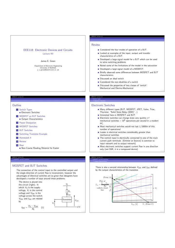
There is also a second relationship between V SW and I SW defined The connection of the control input to the controlled output and by the output characteristics of the transistor. the single direction of current flow is inconvenient, however the advantages of electrical switches are so great that designers have (Point A) developed a number of ways around these problems. (Point B) Plot of The device is placed into I sw = V s − V sw V S the circuit (right). In R L I sw [A] which V S is the supply called a load V i line voltage, V I is the control R L voltage and V SW is the I SW voltage across the switch. V SW and I SW are related Transistor V SW by V I V sw [V] V s (Point C) I SW = V S − V SW 0 V (1) R L 5/ 24 6/ 24

  2. EEE118: Lecture 12 EEE118: Lecture 12 MOSFET an BJT Switches MOSFET an BJT Switches Output Characteristics Output Characteristics Notes on the Output Characteristic Notes on the Output Characteristic II The switch is controlled by V I (which is equal to V BE in this The operating point moves across a non-linear portion of the example). characteristics (it’s a large signal problem) Point C is the “off state” point. The locus - the path - of the operating point across the output characteristics is called the “load line”. It is defined by Point B is the real “on state” point. the load resistance and the supply voltage ( V S ). Point A is the ideal on state point. The load line is straight - no surprise - it represents a As V I is increased, I C will increase and V CE will decrease until resistance as a function of V and I... Ohm’s law. point B is reached. In the region between B and C there is a significant V I The dots on the diagram can be thought of as several product. different operating points but they are not quiescent The designer must keep the transistor at point B or point C conditions as the changes are large compared to the and move between them as fast as possible. non-linearity of the transistor characteristics. 7/ 24 8/ 24 EEE118: Lecture 12 EEE118: Lecture 12 Power Dissipation MOSFET Switches Power Dissipation MOSFET Switches From Lecture 10 the MOSFET behaves like a resistance when “on” (linear region) i.e. at point B. The ZTX653 (from Lecture 10) can dissipate 1 W. Manufactures specify R DS ( on ) . And can carry 2 A... I D is given by, At up to 100 V ( V CE ). V S I D = (2) So it can control 200 W in the load. R L + R DS ( on ) The instantaneous power in the transistor mid-way between B when in the “on” state and C would be 50 W. I D = 0 in the “off” state. Which is sufficient to blow the transistor to pieces. The effect of R DS ( on ) on load power is small (1 – 2% drop). The designer must ensure the transistor switches quickly to keep The effect on the transistor is the average energy in any switching cycle below the permissible limit. More on this in “EEE340: Analogue and Switching Circuits” P = I 2 D ( on ) R DS ( on ) (3) now called “EEE223: Energy Management and Conversion”. which may be significant. 9/ 24 10/ 24 EEE118: Lecture 12 EEE118: Lecture 12 MOSFET Switches BJT Switches MOSFET Switches II BJT Switches When a BJT is fully “on” (i.e. at Point B) the voltage across it is V CE ( sat ) - the saturated on state voltage drop. To ensure the MOSFET is fully “on” the datasheet should be V CE ( sat ) is approximately constant for a constant value of h FE consulted or output characteristics obtained by experiment. A The value of h FE depends on the particular transistor. V GS of 7 – 10V will probably be sufficient to switch the transistor under most circumstances. I C ( on ) = V S − V CE ( sat ) (4) Since the gate is insulated from the source and drain, no R L current is required to maintain the gate drive voltage (MOSFETs have no equivalent of I B ). I C ( off ) = 0 because the leakage is small. Note that the gate has capacitance associated with it and this To be sure the BJT is fully on, the designer must ensure there capacitance complicates transient drive conditions. More in is sufficient base current available. “EEE340: Analogue and Switching Circuits” now called The base current is determined by “EEE223: Energy Management and Conversion”. I B = I C (5) h FE 11/ 24 12/ 24

  3. EEE118: Lecture 12 EEE118: Lecture 12 BJT Switches Switching Transistor Example BJT Switch Design Process Switching Transistor Example: Part One First estimate I C , For the following BJT switching V S I C ≈ V S if V S >> V CE ( sat ) (6) circuit find the, V S R L collector current R L V L then calculate the required base current, load power R L I C V L switch “on” state power loss ∴ min I B = I C V S 4.6 Ω R B = (7) I B range of possible base h FE h FE R L I C V CE currents I B is controlled by V I V BE R B I B maximum value of R B I B = V I − V BE 0 V V CE (8) R B V I V BE V S = 48 V, h FE = 35 – 170, Where V I is the input voltage and V BE is the voltage associated V CE ( sat ) = 0.21 V, V BE ( sat ) = 0.7 V, 0 V with the forward biased base emitter junction (0.7 V). Usually it is V I = 10 V. necessary to make I B several times the minimum value to make the transistor switch properly under all circumstances. 13/ 24 14/ 24 EEE118: Lecture 12 EEE118: Lecture 12 Switching Transistor Example Switching Transistor Example Solution R B R L 10.389 A I B The “on” state or “saturation” large signal model can be drawn (if 0.7 V 9.3 V 47.79 V necessary) + + + + − − 10 V 48 V Bipolar Transistor − 0.21 V − R B R L I C I B V BE ( sat ) V R B V L + + + + − − V I V S V CE ( sat ) − − For the load power, P L = V 2 = (48 − 0 . 21) 2 L = 496 . 49 W (10) R L 4 . 6 For the collector current, apply Ohm’s law to the collector circuit: For the transistor on state power loss, I C = V S − V CE ( sat ) = 48 − 0 . 21 = 10 . 389 A (9) P T = V CE ( sat ) · I C = 0 . 21 · 10 . 389 = 2 . 182 W (11) R L 4 . 6 15/ 24 16/ 24 EEE118: Lecture 12 EEE118: Lecture 12 Switching Transistor Example Switching Transistor Example Switching Transistor Example: Part Two For the minimum I B (need to use max h FE ), What would the new load power and transistor power be if the I C = 10 . 389 BJT was replaced with a MOSFET where R DS ( on ) = 0 . 125 Ω? I B = = 61 . 11 mA (12) h FE ( max ) 170 R G R L I D For the maximum I B (need to use min h FE ), V L R DS ( on ) I C = 10 . 389 V GS V DS + + I B = = 296 . 82 mA (13) V I V S h FE ( min ) 35 − − For the max permissible value of R B (use I B ( max ) ), R B = V I − V BE ( sat ) 10 − 0 . 7 = 296 . 82 × 10 − 3 = 31 . 33 Ω . (14) For the drain current, I B ( max ) V S 48 I D = = 0 . 125 + 4 . 6 = 10 . 158 A (15) Always assume worst case h FE in a switching problem. R DS ( on ) + R L 17/ 24 18/ 24

Download Presentation
Download Policy: The content available on the website is offered to you 'AS IS' for your personal information and use only. It cannot be commercialized, licensed, or distributed on other websites without prior consent from the author. To download a presentation, simply click this link. If you encounter any difficulties during the download process, it's possible that the publisher has removed the file from their server.

Recommend


More recommend