review
play

Review Considered full wave and bridge rectifiers as an extension to - PDF document

EEE118: Lecture 9 Review Considered full wave and bridge rectifiers as an extension to EEE118: Electronic Devices and Circuits the half wave principle Lecture IX Noted that in the full wave circuit the smoothing capacitor is replenished at


  1. EEE118: Lecture 9 Review Considered full wave and bridge rectifiers as an extension to EEE118: Electronic Devices and Circuits the half wave principle Lecture IX Noted that in the full wave circuit the smoothing capacitor is replenished at double the line frequency James E. Green Observed that the output voltage polarity available is only a function of where the reference is placed Department of Electronic Engineering Discussed the differences between three phase and single University of Sheffield phase systems more fully. j.e.green@sheffield.ac.uk Concluded the section on linear power supplies with a review of the circuits. Introduced stabilisation and regulation of power supplies. Briefly noted the existence of series and shunt regulators Discussed the usefulness of the Zener diode as a shunt regulator 2/ 20 1/ 20 EEE118: Lecture 9 EEE118: Lecture 9 EEE118. “Electronic Devices and Circuits” Outline Part 2 1 Impact Ionisation Lecture 9. (Today) A last word on Diode Regulators 2 Zener Diode from a Circuit Perspective Lecture 10. Small Signals in Diode Circuits & Introduction to 3 Zener Diode Regulator Design Method Transistors The Regulator’s Effect on Ripple Lectures 11. & 12. Transistor Characteristics Graphs & Switching Applications of Transistors 4 Homework 3 Lectures 13. & 14. Transistor circuits for Switching AC & 5 All Signals Great and Small Inductive Loads. & Amplifying Applications of Transistors Lectures 15. Two Single Transistor Amplifier Circuits & Small 6 Large Signal Diode Circuit Example Signal Modelling 7 Review Lectures 16 & 17. Operational Amplifiers Lectures 18 & 19. Review and Past Exam Run-through. 8 Bear 3/ 20 4/ 20 EEE118: Lecture 9 EEE118: Lecture 9 Impact Ionisation Impact Ionisation Zener Diodes - Impact ionisation
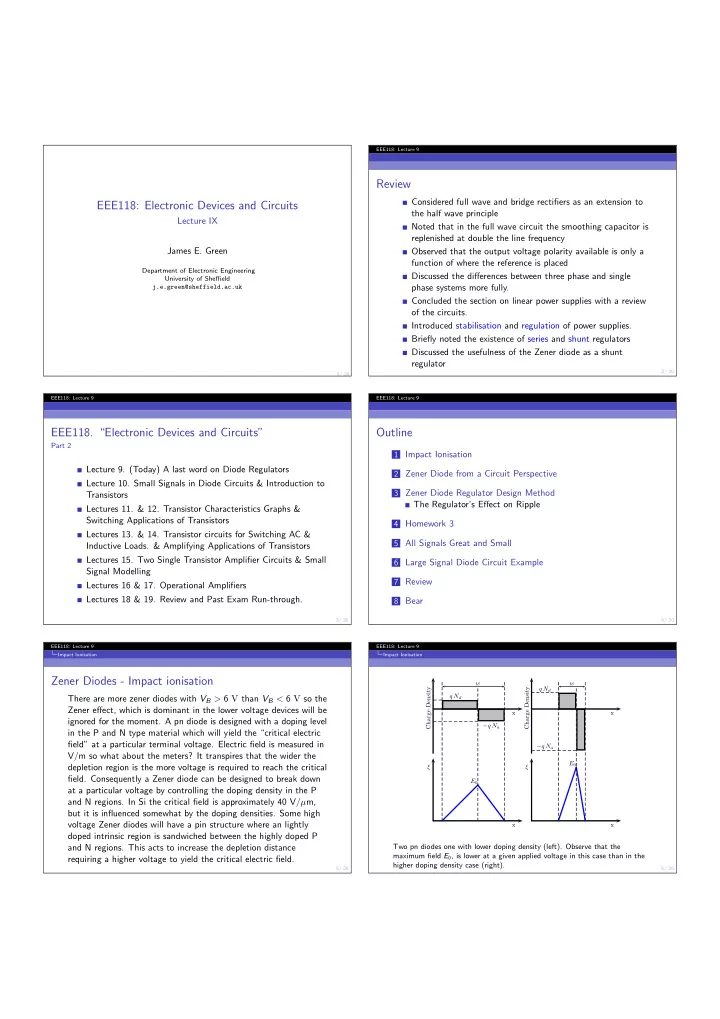
 w w Charge Density Charge Density q N d q N d There are more zener diodes with V B > 6 V than V B < 6 V so the Zener effect, which is dominant in the lower voltage devices will be x x ignored for the moment. A pn diode is designed with a doping level − q N a in the P and N type material which will yield the “critical electric field” at a particular terminal voltage. Electric field is measured in − q N a V/m so what about the meters? It transpires that the wider the E 0 depletion region is the more voltage is required to reach the critical ξ ξ field. Consequently a Zener diode can be designed to break down E 0 at a particular voltage by controlling the doping density in the P and N regions. In Si the critical field is approximately 40 V/ µ m, but it is influenced somewhat by the doping densities. Some high voltage Zener diodes will have a pin structure where an lightly x x doped intrinsic region is sandwiched between the highly doped P and N regions. This acts to increase the depletion distance Two pn diodes one with lower doping density (left). Observe that the maximum field E 0 , is lower at a given applied voltage in this case than in the requiring a higher voltage to yield the critical electric field. higher doping density case (right). 5/ 20 6/ 20

  2. EEE118: Lecture 9 EEE118: Lecture 9 Zener Diode from a Circuit Perspective Zener Diode Regulator Design Method Zener Diodes from a Circuit Perspective A Zener Diode Shunt Regulator Circuit Since a Zener diode is normally used in reverse bias, it will be R 1 I T In this circuit V i is the output assumed that the the cathode will be positive w.r.t anode I L I Z from any of the rectifier from now on. + V i D 1 R L V o circuits that have been Zener diodes are only effective regulators if they are biased − discussed in this course. above their reverse breakdown voltage. Once the diode has broken down in a reverse direction, an The output voltage V o will be close to V B provided the diode increase in reverse bias ∆ V will lead to an increase in reverse is biased above its breakdown voltage. If V C − A > V B the current ∆ I current is always greater than zero. The ratio of the small change in V against the small change in I is the dynamic or small signal 1 resistance of the reverse Assume the load current, I L , is constant but V i is variable - due to ripple or utility variations. biased diode. It is variable and depends on the biasing A reduction in V i of ∆ V i will cause a reduction in voltage conditions. It cannot be computed by dividing the breakdown across R 1 of ∆ V i and hence a reduction in the output voltage. voltage by the current. It is the change in V and the change However the falling output voltage acts to slightly switch off in I over a small portion of the breakdown characteristic that the Zener diode causing the Zener current, I Z , to fall by just is important. dv/di. enough to prevent V o changing. 1 small and large signals will be treated fully in semester two. 7/ 20 8/ 20 EEE118: Lecture 9 EEE118: Lecture 9 Zener Diode Regulator Design Method Zener Diode Regulator Design Method The reduction in the total current I T due to the falling Consider the conditions that are most likely to cause the voltage drop across R 1 is compensated by a similar reduction regulator to switch off i.e. minimum input voltage and in I Z such that I L (and therefore V o ) are unaffected. maximum load current; find a value for R 1 . The maximum Similarly if V i remains constant but I L changes the increasing required load current and minimum required Zener current I L tends to lower V o . A small decrease in V o tends to switch must be able to flow even when the input voltage is at a off the Zener diode slightly, reducing its current and alowing minimum. I L to increase such that V o remains unchanged. V i min − V o = I L max + I Z min (1) Design Approach, R 1 Work out or choose, based on your knowledge of the load, the If the value of R 1 is larger than that given by (1), there would be maximum load current, I L . insufficient current under the worst case of input voltage to satisfy Choose a Zener diode based on the required output voltage the requirements of the load and the regulator. Therefore (1) V o (e.g. BZX55C25 - 25 V) represents the largest acceptable value of R 1 . Of course if R 1 is made smaller than this value its power dissipation will be Use the diode’s manufacturers data sheet to find the minimum current required for proper operation (smallest I Z unnecessarily high. that still yields the correct breakdown voltage). 9/ 20 10/ 20 EEE118: Lecture 9 EEE118: Lecture 9 Zener Diode Regulator Design Method Zener Diode Regulator Design Method The Regulator’s Effect on Ripple The Regulator’s Effect on Ripple R 1 Calculate the worst case power dissipation in R 1 . (hint: Max In the ripple equivalent circuit only the effect of the small input voltage, full load current) v in r r d v o ripple is considered, hence the Calculate the worst case power dissipation in the Zener diode input is AC. The DC has been (hint: Max input voltage, no load current). Check the Zener neglected. you chose is capable of dissipating the required power, if not select a higher power Zener diode. The output ripple voltage, v o is obviously a potential division of Effect on the ripple, the input ripple voltage v in r in the ratio of R 1 and the small signal To calculate the effect of the Zener diode regulator on the (dynamic) resistance of the Zener diode. The load resistance (if it ripple an equivalent circuit can be used which models the is connected) appears in parallel with the dynamic resistance of the small changes in Zener resistance that occur to due small Zener and the two may be paralleled using the usual formula. fluctuations in the input voltage (or load current). Hence the value of v o calculated without the load is the worst case If the regulator has been well designed the diode will be ripple voltage. If r d is lower than R 1 (almost always true) there can broken down in the reverse direction. From the perspective of be a significant reduction in output ripple. Limitations, the ripple signal the diode can be thought of as a small signal The voltage is not adjustable. (or dynamic) resistance which is equal to the inverse of the The Zener and R 1 may have high power dissipation. slope of the tangent of the breakdown characteristic at the The dynamic resistance of the Zener is low it is not as low as operating point. transistor based linear regulators. 11/ 20 12/ 20

Download Presentation
Download Policy: The content available on the website is offered to you 'AS IS' for your personal information and use only. It cannot be commercialized, licensed, or distributed on other websites without prior consent from the author. To download a presentation, simply click this link. If you encounter any difficulties during the download process, it's possible that the publisher has removed the file from their server.

Recommend


More recommend