Introduction to Synchronous Sequential Introduction to Synchronous - - PDF document

introduction to synchronous sequential introduction to
SMART_READER_LITE
LIVE PREVIEW

Introduction to Synchronous Sequential Introduction to Synchronous - - PDF document

Introduction to Synchronous Sequential Introduction to Synchronous Sequential Circuits Circuits 1 Zvi Kohavi and Niraj K. Jha Sequential Circuits and Finite Sequential Circuits and Finite- -state state Machines Machines Machines


slide-1
SLIDE 1

Introduction to Synchronous Sequential Introduction to Synchronous Sequential Circuits Circuits

Zvi Kohavi and Niraj K. Jha

1

Sequential Circuits and Finite Sequential Circuits and Finite-

  • state

state Machines Machines Machines Machines

Sequential circuit: its outputs a function of external inputs as well as stored i f ti information Finite-state machine (FSM): abstract model to describe the synchronous sequential machine and its spatial counterpart, the iterative network Serial binary adder example: block diagram, addition process, state table and state diagram

A B 00/0 01/1 11/0 01/0 10/0

2

A B 01/1 10/1 00/1 10/0 11/1

slide-2
SLIDE 2

State Assignment State Assignment State Assignment State Assignment

Device with two states capable of storing information: delay element with i t Y d t t input Y and output y

  • Two states: y = 0 and y = 1
  • Since the present input value Y of the delay element is equal to its next
  • utput value: the input value is referred to as the next state of the delay
  • utput value: the input value is referred to as the next state of the delay

– Y(t) = y(t+1)

Example: assign state y = 0 to state A of the adder and y = 1 to B

  • The value of y at ti corresponds to the value of the carry generated at ti-1
  • Process of assigning the states of a physical device to the states of the

serial adder: called state assignment

  • Output value y: referred to as the state variable
  • Transition/output table for the serial adder:

Y = x1x2 + x1y + x2y z = x1 x2 y

Full adder z x1 x2

3

adder y C0 Delay Y

FSM: Definitions FSM: Definitions FSM: Definitions FSM: Definitions

FSMs: whose past histories can affect their future behavior in only a finite b f number of ways

  • Serial adder: its response to the signals at time t is only a function of

these signals and the value of the carry at t-1 Thus its input histories can be grouped into just two classes: those – Thus, its input histories can be grouped into just two classes: those resulting in a 1 carry and those resulting in a 0 carry at t

  • Thus, every finite-state machine contains a finite number of memory

devices: which store the information regarding the past input history devices: which store the information regarding the past input history

4

slide-3
SLIDE 3

Synchronous Sequential Machines Synchronous Sequential Machines Synchronous Sequential Machines Synchronous Sequential Machines

Combinational z1 x1 xl zm Combinational logic y1 Y1 yk Yk y2 Y2

Input variables: {x1, x2, .., xl} Input configuration, symbol, pattern or vector: ordered l-tuple of 0’s and 1’s

``Memory’’ devices

Input alphabet: set of p = 2l distinct input patterns

  • Thus, input alphabet I = {I1, I2, .., Ip}
  • Example: for two variables x1 and x2

p

1 2

– I = {00, 01, 10, 11}

Output variables: {z1, z2, .., zm} Output configuration symbol pattern or vector: ordered m-tuple of 0’s and 1’s

5

Output configuration, symbol, pattern or vector: ordered m-tuple of 0 s and 1 s Output alphabet: set of q = 2m distinct output patterns

  • Thus, output alphabet O = {O1, O2, .., Oq}

Synchronous Sequential Machines Synchronous Sequential Machines (Contd ) (Contd ) (Contd.) (Contd.)

Set of state variables: {y1, y2, .., yk} Present state: combination of values at the outputs of k memory elements Set S of n = 2k k-tuples: entire set of states S = {S1, S2, .., Sn} Next state: values of Y’s Next state: values of Y s Synchronization achieved by means of clock pulses feeding the memory devices Initial state: state of the machine before the application of an input pp p sequence to it Final state: state of the machine after the application of the input

6

Final state: state of the machine after the application of the input sequence

slide-4
SLIDE 4

Memory Elements and Their Excitation Memory Elements and Their Excitation Functions Functions Functions Functions

To generate the Y’s: memory devices must be supplied with appropriate i t l input values

  • Excitation functions: switching functions that describe the impact of xi’s

and yj’s on the memory-element input Excitation table: its entries are the values of the memory element inputs

  • Excitation table: its entries are the values of the memory-element inputs

Most widely used memory elements: flip-flops, which are made of latches

  • Latch: remains in one state indefinitely until an input signals directs it to do
  • therwise

Set-reset of SR latch:

1 y S R (a) Block diagram. y R y S y

7

S y (b) NOR latch. R y (c) NAND latch.

SR SR Latch (Contd.) Latch (Contd.)

Excitation characteristics and requirements: Clocked SR latch: all state changes synchronized to clock pulses

  • Restrictions placed on the length and frequency of clock pulses: so that

Restrictions placed on the length and frequency of clock pulses: so that the circuit changes state no more than once for each clock pulse

y S R y Clock C

8

R (a) Block diagram. y S y (b) Logic diagram. Clock C

slide-5
SLIDE 5

Trigger or Trigger or T Latch Latch

Value 1 applied to its input triggers the latch to change state Excitations requirements: y(t+1) = Ty’(t) + T’y(t)

9

= T y(t)

The The JK JK Latch Latch

Unlike the SR latch, J = K = 1 is permitted: when it occurs, the latch acts lik t i d it h t th l t t t like a trigger and switches to the complement state Excitation requirements:

10

slide-6
SLIDE 6

The The D Latch Latch

The next state of the D latch is equal to its present excitation: y(t+1) = D(t)

11

Clock Timing Clock Timing

Clocked latch: changes state only in synchronization with the clock pulse d th d i h f th l k l and no more than once during each occurrence of the clock pulse Duration of clock pulse: determined by circuit delays and signal propagation time through the latches

  • Must be long enough to allow latch to change state, and
  • Short enough so that the latch will not change state twice due to the same

excitation

Excitation of a JK latch within a sequential circuit:

  • Length of the clock pulse must allow the latch to generate the y’s
  • But should not be present when the values of the y’s have propagated

through the combinational circuit

12

slide-7
SLIDE 7

Master Master-

  • slave Flip

slave Flip-

  • flop

flop

Master-slave flip-flop: a type of synchronous memory element that li i t th ti i bl b i l ti it i t f it eliminates the timing problems by isolating its inputs from its

  • utputs

Master-slave SR flip-flop: Master-slave JK flip-flop: since master-slave SR flip-flop suffers from the problem that both its inputs cannot be 1 it can be converted to a problem that both its inputs cannot be 1, it can be converted to a JK flip-flip

S R y y SR Master- slave 1 J K

13

Master Master-

  • slave JK Flip

slave JK Flip-

  • flop with Additional

flop with Additional Inputs Inputs Inputs Inputs

Direct set and clear inputs: override regular input signals and clock

  • To set the slave output to 0: make set = 1 and clear = 0
  • To set the slave output to 1: make set = 0 and clear = 1
  • Assigning 0 to both set and clear: not allowed
  • Assigning 1 to both set and clear: normal operation
  • Useful in design of counters and shift registers

14

slide-8
SLIDE 8

1’s Catching and 0’s Catching 1’s Catching and 0’s Catching

SR and JK flip-flops suffer from 1’s catching and 0’s catching

S y SR Master- l 1 J

Master latch is transparent when the clock is high

R y slave 0 K

Master latch is transparent when the clock is high

  • When the output of the slave latch is at 0 and the J input has a static-0

hazard (a transient glitch to 1) after the clock has gone high: then the master latch catches this set condition master latch catches this set condition – It then passes the 1 to the slave latch when the clock goes low

  • Similarly, when the output of the slave latch is at 1 and the K input has a

static-0 hazard after the clock has gone high: then the master latch static 0 hazard after the clock has gone high: then the master latch catches this reset condition – It then passes the 0 to the slave latch when the clock goes low

15

D flip flip-

  • flop

flop

Master-slave D flip-flop avoids the above problem: even when a static h d t th D i t h th l k i hi h th t t f hazard occurs at the D input when the clock is high, the output of the master latch reverts to its old value when the glitch goes away

J y 1 D JK K y y 1 JK Master- slave

16

slide-9
SLIDE 9

Edge Edge-

  • triggered Flip

triggered Flip-

  • flop

flop

Positive (negative) edge-triggered D flip-flip: stores the value at the D input h th l k k 0 > 1 (1 > 0) t iti when the clock makes a 0 -> 1 (1 -> 0) transition

  • Any change at the D input after the clock has made a transition does not

have any effect on the value stored in the flip-flop

A negative edge-triggered D flip-flop:

  • When the clock is high, the output of the bottommost (topmost) NOR gate

i D (D) h h S R i f h l h i i is at D’ (D), whereas the S-R inputs of the output latch are at 0, causing it to hold previous value

  • When the clock goes low, the value from the

b tt t (t t) NOR t t t f d bottommost (topmost) NOR gate gets transferred as D (D’) to the S (R) input of the output latch – Thus, output latch stores the value of D If th i h i th l f th D

Clock R y

  • If there is a change in the value of the D

input after the clock has made its transition, the bottommost NOR gate attains value 0

Clock S y

17

– However, this cannot change the SR inputs of the output latch

D

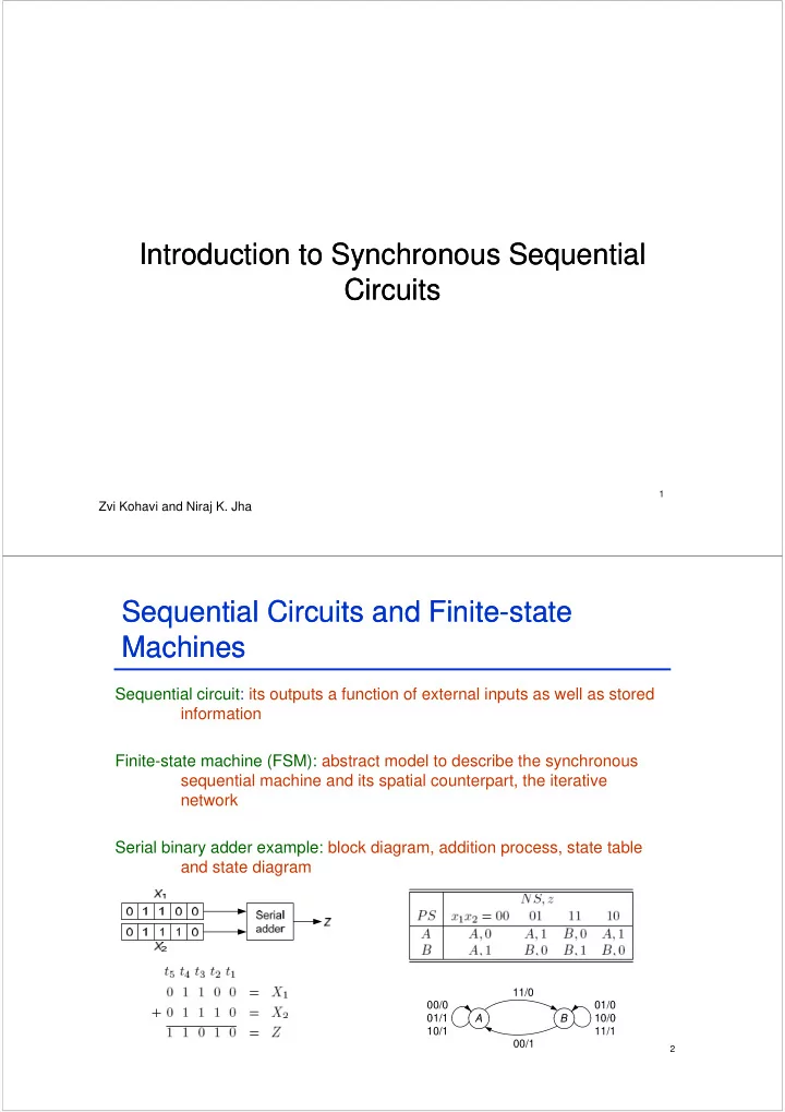
Synthesis of Synchronous Sequential Synthesis of Synchronous Sequential Circuits Circuits Circuits Circuits

Main steps:

f f 1. From a word description of the problem, form a state diagram or table 2. Check the table to determine if it contains any redundant states

  • If so, remove them (Chapter 10)

3. Select a state assignment and determine the type of memory elements 4. Derive transition and output tables 5. Derive an excitation table and obtain excitation and output functions from their ti t bl respective tables 6. Draw a circuit diagram

18

slide-10
SLIDE 10

Sequence Detector Sequence Detector

One-input/one-output sequence detector: produces output value 1 every ti 0101 i d t t d l time sequence 0101 is detected, else 0

  • Example: 010101 -> 000101

State diagram and state table: Transition and output tables:

19

Sequence Detector (Contd.) Sequence Detector (Contd.)

Excitation and output maps: z = xy1y2’ y1 = x’y1y2 + xy1’y2 + xy1y2’ y2 = y1y2’ + x’y1’ + y1’y2 Logic diagram:

20

slide-11
SLIDE 11

Sequence Detector (Contd.) Sequence Detector (Contd.)

Another state assignment: z = xy1y2 Y1 = x’y1y2’ + xy2 Y2 = x’

21

Binary Counter Binary Counter

One-input/one-output modulo-8 binary counter: produces output value 1 for i hth i t 1 l every eighth input 1 value State diagram and state table:

0/0 0/0 1/1 1/0 0/0 S0 S S 0/0 1/0 1/0 S7 S6 S2 S1 0/0 S3 S5 S4 1/0 1/0 1/0 1/0 0/0 0/0 0/0 0/0 22

slide-12
SLIDE 12

Binary Counter (Contd.) Binary Counter (Contd.)

Transition and output tables: Excitation table for T Excitation table for T flip-flops and logic diagram: T1 = x T2 = xy1

23

T3 = xy1y2 z = xy1y2y3

Implementing the Counter with Implementing the Counter with SR SR Flip Flip-

  • flops

flops flops flops

Transition and output tables: Excitation table for SR

Cell 1 Cell 3 Cell 2

Excitation table for SR flip-flops and logic diagram:

  • Trivially extensible to

S3 R3 y3 1 y3 S1 R1 x y1 1 y1 S2 R2 y2 1 y2

modulo-16 counter

S1 = xy1’

y3 y1 y2 z

1

y1 R1 = xy1 S2 = xy1y2’ R = xy y

24

R2 = xy1y2 S3 = xy1y2y3’ R3 = z = xy1y2y3

slide-13
SLIDE 13

Parity Parity-

  • bit Generator

bit Generator

Serial parity-bit generator: receives coded messages and adds a parity bit t bit to every m-bit message

  • Assume m = 3 and even parity

State diagram and state table:

A 0,1/0 0,1/1 B C 0/0 0/0 0,1/0 1/0 0/0 0,1/1 D 0/0 0/0 0/0 1/0 E 0/0 1/0

J1 = y2 K1 = y2’

0/0 1/0 F G 0/0 1/0 1

y2 J2 = y1’ K2 = y1 J3 = xy1’ + xy2

25

J3 xy1 + xy2 K3 = x + y2’ z = y2’y3

Sequential Circuit as a Control Element Sequential Circuit as a Control Element

Control element: streamlines computation by providing appropriate control i l signals Example: digital system that computes the value of (4a + b) modulo 16

  • a b: four bit binary number
  • a, b: four-bit binary number
  • X: register containing four flip-flops
  • x: number stored in X

R i t b l d d ith ith b +

  • Register can be loaded with: either b or a + x
  • Addition performed by: a four-bit parallel adder
  • K: modulo-4 binary counter, whose output L equals 1 whenever the count

is 3 modulo 4 is 3 modulo 4

ADD b (4a + b)16 X a 4 4 4 4 k2 L x K k1 4

26

L Sequential circuit M u Initiate z

slide-14
SLIDE 14

Example (Contd.) Example (Contd.)

Sequential circuit M:

  • Input u: initiates computation
  • Input L: gives the count of K
  • Outputs:

, , , z

  

  • When = 1: contents of b transferred to X
  • When = 1: values of x and a added and transferred back to X
  • When = 1: count of K increased by 1

 

  • z = 1: whenever final result available in X

b 4 ADD x (4a + b)16 X K k1 a 4 4 4 4 k2 L S ti l i it M Initiate K 4

27

Sequential circuit M u z

Example (Contd.) Example (Contd.)

Sequential circuit M:

  • K, u, z: initially at 0
  • When u = 1: computation starts by setting = 1

– Causes b to be loaded into X

  • To add a to x: set = 1 and = 1 to keep track of the number of times a

has been added to x

  • After four such additions: z = 1 and the computation is complete

At thi i t K 0 t b d f th t t ti

 

  • At this point: K = 0 to be ready for the next computation

State diagram:

b ADD b (4a + b)16 X a 4 4 4 4 A u = 0 00

  • /z = 1

u = 1 k2 L x K k1 4 B D 10 01 u = 1

  • / = 1

28

Sequential circuit M u Initiate z = 1 11 L = 0/ = 1 C = 1 L = 1/ = 1

slide-15
SLIDE 15

Example (Contd.) Example (Contd.)

State assignment, transition table, maps and logic diagram:

A u = 0 00

  • /z = 1

u = 1

1 y1 y2 u 1 y1 y2 PS NS y1y2 Y1Y2 00 11 0u 01

B D 10 01 C

  • / = 1

1 1 1 1 L 1 Y1 Y2 00 1L 11 10 11 01

= 1 11 L = 0/ = 1 C = 1 L = 1/ = 1

z D1 y1 Y1 (b) Maps for Y1 and Y2. (a) Transition table. Clock y1 ,

= y1’y2 = = y1y2 z = y1y2’

 

y2 Y2 D2 Cl k L y2

y1y2 Y1 = y2 Y2 = y1’y2 + uy1’ + L’y2

29

u Clock y2 Clock (c) Logic diagram.