
SLIDE 1
1
1
Synchronous Logic
- M. Sachdev
- Dept. of Electrical & Computer Engineering
University of Waterloo
ECE 223 Digital Circuits and Systems
2
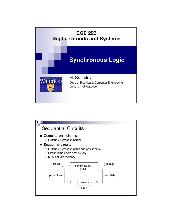
Sequential Circuits
Combinational circuits
Output = f (present inputs)
Sequential circuits
Output = f (present inputs and past inputs) Circuit remembers past history Must contain memory
inputs k n outputs present state next state combinational circuit memory m m state