
SLIDE 1
1
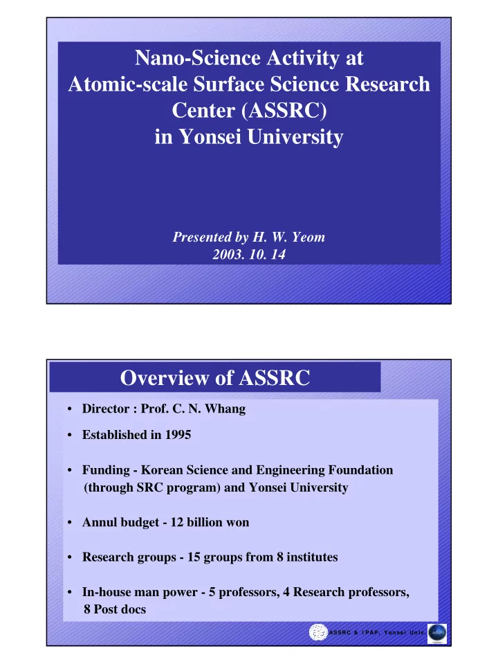
Nano-Science Activity at Atomic-scale Surface Science Research Center (ASSRC) in Yonsei University
Presented by H. W. Yeom
- 2003. 10. 14
Overview of ASSRC
- Director : Prof. C. N. Whang
- Established in 1995
- Funding - Korean Science and Engineering Foundation
(through SRC program) and Yonsei University
- Annul budget - 12 billion won
- Research groups - 15 groups from 8 institutes
- In-house man power - 5 professors, 4 Research professors,
8 Post docs
ASSRC & I PAP, Y on se i U n iv.