SLIDE 4
Verilog: alucontrol
module alucontrol(input [1:0] aluop, input [5:0] funct,
- utput reg [2:0] alucont);
always @(*) case(aluop) 2'b00: alucont <= 3'b010; // add for lb/sb/addi 2'b01: alucont <= 3'b110; // sub (for beq) default: case(funct) // R-Type instructions 6'b100000: alucont <= 3'b010; // add (for add) 6'b100010: alucont <= 3'b110; // subtract (for sub) 6'b100100: alucont <= 3'b000; // logical and (for and) 6'b100101: alucont <= 3'b001; // logical or (for or) 6'b101010: alucont <= 3'b111; // set on less (for slt) default: alucont <= 3'b101; // should never happen endcase endcase endmodule
Verilog: alu
module alu #(parameter WIDTH = 8) (input [WIDTH-1:0] a, b, input [2:0] alucont,
- utput reg [WIDTH-1:0] result);
wire [WIDTH-1:0] b2, sum, slt; assign b2 = alucont[2] ? ̃b:b; assign sum = a + b2 + alucont[2]; // slt should be 1 if most significant bit of sum is 1 assign slt = sum[WIDTH-1]; always@(*) case(alucont[1:0]) 2'b00: result <= a & b; 2'b01: result <= a ¦ b; 2'b10: result <= sum; 2'b11: result <= slt; endcase endmodule
Verilog: regfile
module regfile #(parameter WIDTH = 8, REGBITS = 3) (input clk, input regwrite, input [REGBITS-1:0] ra1, ra2, wa, input [WIDTH-1:0] wd,
- utput [WIDTH-1:0] rd1, rd2);
reg [WIDTH-1:0] RAM [(1<<REGBITS)-1:0]; // three ported register file // read two ports (combinational) // write third port on rising edge of clock // register 0 is hardwired to 0 always @(posedge clk) if (regwrite) RAM[wa] <= wd; assign rd1 = ra1 ? RAM[ra1] : 0; assign rd2 = ra2 ? RAM[ra2] : 0; endmodule
Verlog: Other stuff
module zerodetect #(parameter WIDTH = 8) (input [WIDTH-1:0] a,
assign y = (a==0); endmodule module flop #(parameter WIDTH = 8) (input clk, input [WIDTH-1:0] d,
- utput reg [WIDTH-1:0] q);
always @(posedge clk) q <= d; endmodule module flopen #(parameter WIDTH = 8) (input clk, en, input [WIDTH-1:0] d,
- utput reg [WIDTH-1:0] q);
always @(posedge clk) if (en) q <= d; endmodule
module flopenr #(parameter WIDTH = 8) (input clk, reset, en, input [WIDTH-1:0] d,
- utput reg [WIDTH-1:0] q);
always @(posedge clk) if (reset) q <= 0; else if (en) q <= d; endmodule module mux2 #(parameter WIDTH = 8) (input [WIDTH-1:0] d0, d1, input s,
assign y = s ? d1 : d0; endmodule module mux4 #(parameter WIDTH = 8) (input [WIDTH-1:0] d0, d1, d2, d3, input [1:0] s,
- utput reg [WIDTH-1:0] y);
always @(*) case(s) 2'b00: y <= d0; 2'b01: y <= d1; 2'b10: y <= d2; 2'b11: y <= d3; endcase endmodule
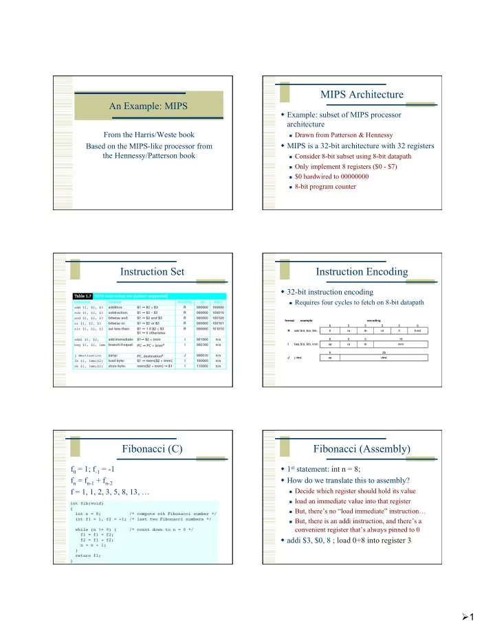
MIPS Microarchitecture
Multicycle µarchitecture from Patterson & Hennessy
module datapath #(parameter WIDTH = 8, REGBITS = 3) (input clk, reset, input [WIDTH-1:0] memdata, input alusrca, memtoreg, iord, pcen, regwrite, regdst, input [1:0] pcsource, alusrcb, input [3:0] irwrite, input [2:0] alucont,
- utput zero,
- utput [31:0] instr,
- utput [WIDTH-1:0] adr, writedata);
// the size of the parameters must be changed to match the WIDTH parameter localparam CONST_ZERO = 8'b0; localparam CONST_ONE = 8'b1; wire [REGBITS-1:0] ra1, ra2, wa; wire [WIDTH-1:0] pc, nextpc, md, rd1, rd2, wd, a, src1, src2, aluresult, aluout, constx4; // shift left constant field by 2 assign constx4 = {instr[WIDTH-3:0],2'b00}; // register file address fields assign ra1 = instr[REGBITS+20:21]; assign ra2 = instr[REGBITS+15:16]; mux2 #(REGBITS) regmux(instr[REGBITS+15:16], instr[REGBITS+10:11], regdst, wa);
Verilog: Datapath 1