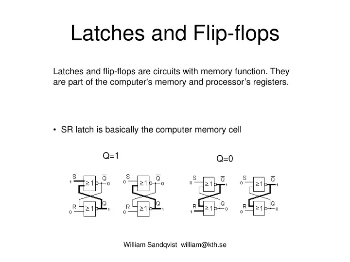
latches and flip flops
play

Latches and Flip-flops Latches and flip-flops are circuits with - PowerPoint PPT Presentation

Latches and Flip-flops Latches and flip-flops are circuits with memory function. They are part of the computer's memory and processors registers. SR latch is basically the computer memory cell Q=1 Q=0 William Sandqvist william@kth.se


  1. Latches and Flip-flops Latches and flip-flops are circuits with memory function. They are part of the computer's memory and processor’s registers. • SR latch is basically the computer memory cell Q=1 Q=0 William Sandqvist william@kth.se

  2. SR latch with two NOR-gates If S = 1 and R = 0 it causes the upper Q=1 gate to "0". The lower gate inputs then becomes 00 and it’s output Q = 1. Since the upper gate now get "1" from both inputs, it now does not matter if S = 0. Q remains locked to output "1". If R = 1 and S = 0 it causes the lower gate Q=0 to "0". Output is Q = 0. The upper gate inputs becomes 00 giving "1" at it’s output and "1" at the input of the lower gate. Since the lower gate now get "1" from both inputs, it now does not matter if R = 0. Q remains unlocked to "0". William Sandqvist william@kth.se

  3. Ex 9.1 Complete the timing diagram for the output signals Q and . Q The distance between the pulses is much longer than the gate delay. (Hint, what is the locking input signal for NOR gates?) William Sandqvist william@kth.se

  4. Ex 9.1 Complete the timing diagram for the output signals Q and . Q The distance between the pulses is much longer than the gate delay. (Hint, what is the locking input signal for NOR gates?) William Sandqvist william@kth.se

  5. Ex 9.1 Complete the timing diagram for the output signals Q and . Q The distance between the pulses is much longer than the gate delay. (Hint, what is the locking input signal for NOR gates?) William Sandqvist william@kth.se

  6. Ex 9.1 Complete the timing diagram for the output signals Q and . Q The distance between the pulses is much longer than the gate delay. (Hint, what is the locking input signal for NOR gates?) William Sandqvist william@kth.se

  7. Ex 9.1 Complete the timing diagram for the output signals Q and . Q The distance between the pulses is much longer than the gate delay. (Hint, what is the locking input signal for NOR gates?) William Sandqvist william@kth.se

  8. Ex 9.1 Complete the timing diagram for the output signals Q and . Q The distance between the pulses is much longer than the gate delay. (Hint, what is the locking input signal for NOR gates?) William Sandqvist william@kth.se

  9. Ex 9.1 Complete the timing diagram for the output signals Q and . Q The distance between the pulses is much longer than the gate delay. (Hint, what is the locking input signal for NOR gates?) William Sandqvist william@kth.se

  10. Ex 9.1 Complete the timing diagram for the output signals Q and . Q The distance between the pulses is much longer than the gate delay. (Hint, what is the locking input signal for NOR gates?) William Sandqvist william@kth.se

  11. Ex 9.1 Complete the timing diagram for the output signals Q and . Q The distance between the pulses is much longer than the gate delay. (Hint, what is the locking input signal for NOR gates?) For S = 1 and R = 1 the latch does not work, the outputs will then not be each others inverses, but both will be 0. William Sandqvist william@kth.se

  12. SR-latch characteristic table same forbidden A short "pulse" S = 1 "sets" the latch circuit and a short "pulse" R = 1 "resets" it. As long as the S = 0 and R = 0, the latch retains its value In the characteristic table the input combination S = 1 and R = 1 is forbidden!. For this combination would both gates outputs become "0" at the same time. For the other input combinations it applies that the outputs are each other's inverses. If you want to guarantee that the "other" output is always inverted, you have to "ban" the forbidden input signal combination. William Sandqvist william@kth.se

  13. Edge triggered Flip-flop In digital technology there is a distinction between simple latches and clocked flip-flops. ? The limitation of the simple latch is that one can not enter a new value to the input while reading the output. The high speed of electronic circuits has made it necessary to develop more sophisticated circuits. Edge-triggered D flip-flop. D input is the data input, C input is the clock pulse input, hence the designation CP. The control input C has an edge trigger sign, a triangle. When the C input is reached by a positive edge, ie. the short period of time when C goes from "0" to "1", the D-input value is copied to the output Q. The output value is then locked until a new edge of the clock pulse is received. William Sandqvist william@kth.se

  14. Synchronization with D flip-flops • D flip-flop used to synchronize the signal flow between the different parts of the computer. D flip-flops are used to stop the race between signals for the value to become stable. (Compare with the tollbooth that stops the cars). William Sandqvist william@kth.se

  15. Synchronization with D flip-flops • D flip-flop used to synchronize the signal flow between the different parts of the computer. D flip-flops are used to stop the race between signals for the value to become stable. (Compare with the tollbooth that stops the cars). ? William Sandqvist william@kth.se

  16. Synchronization with D flip-flops • D flip-flop used to synchronize the signal flow between the different parts of the computer. D flip-flops are used to stop the race between signals for the value to become stable. (Compare with the tollbooth that stops the cars). ? ! William Sandqvist william@kth.se

  17. (9.4) Draw output Q in this timing diagram William Sandqvist william@kth.se

  18. (9.4) Draw output Q in this timing diagram William Sandqvist william@kth.se

  19. T-function Q T=0 Same T=1 Change, Toggle Q Q Sometimes this symbol of T-function is used. Q The T-flip-flop. William Sandqvist william@kth.se

  20. Ex 9.3 Draw the timing diagram for the output Q of the D flip-flop. William Sandqvist william@kth.se

  21. Ex 9.3 Draw the timing diagram for the output Q of the D flip-flop. William Sandqvist william@kth.se

  22. Ex 9.3 Draw the timing diagram for the output Q of the D flip-flop. William Sandqvist william@kth.se

  23. Ex 9.3 Draw the timing diagram for the output Q of the D flip-flop. William Sandqvist william@kth.se

  24. Ex 9.3 Draw the timing diagram for the output Q of the D flip-flop. William Sandqvist william@kth.se

  25. Ex 9.3 Draw the timing diagram for the output Q of the D flip-flop. William Sandqvist william@kth.se

  26. Ex 9.3 Draw the timing diagram for the output Q of the D flip-flop. William Sandqvist william@kth.se

  27. Ex 9.5 JK flip-flop was an older type of "universal flip-flop". Show how it can be used as the T-flip-flop and as D-flip-flop. Characteristic table same toggle William Sandqvist william@kth.se

  28. Ex 9.5 JK flip-flop can be used as the T flip-flop or D flip-flop. (When flip-flops are connected to each other there are usually the inverted outputs available, you will then not require the inverter to make the JK flip flop to D flip-flop.) William Sandqvist william@kth.se

  29. Ex 9.6 What is the maximum clock frequency that can be used to the circuit in the figure without the risk of failure? Suppose that t s = 20 ns t h = 5 ns t pd = 30 ns William Sandqvist william@kth.se

  30. Ex 9.6 t s = 20 ns t h = 5 ns t pd = 30 ns William Sandqvist william@kth.se

  31. Ex 9.6 t s = 20 ns t h = 5 ns t pd = 30 ns = + T t t pd s 1 1 1 = = = = f 20 MHz [ ] + + T t t ( 20 30 ) ns pd s William Sandqvist william@kth.se

  32. William Sandqvist william@kth.se

  33. Asynchronous binary counter The figure above shows a binary counter with three flip-flops, the counting cycle has eight states so it is a modulo-8 counter. The counter is built of T-flip-flops, as they all have T = 1 they "toggles" at each clock pulse. The first flip-flop Q 0 "toggles" every clock pulse. The flip-flop Q 1 is clocked by the first flip-flop. It will therefore only "toggle" for every other clock pulse. The third flip-flop Q 2 will "toggle" for every other every other clock pulse. According to the binary table, the counter is counting in binary code. ( Q 2 Q 1 Q 0 : 000 001 010 011 100 101 110 111 000 ... ). William Sandqvist william@kth.se

  34. Asynchronous counter weakness Asynchronous counter has the simplest possible structure. Since the clock pulses are routed through the flip-flops so they can not change state on exactly the same time. If you read the binary code on the outputs of flip-flops during the transition, then “any” code can appear for a short time! The flip-flops changes output one after another and you could say that the clock pulse "ripples" through the flip-flops (asynchronous counters are therefore sometimes called ripple counters ). This problem has been solved with the synchronous counters . William Sandqvist william@kth.se

  35. BV 7.5 Given a 100-MHz clock signal, derive a circuit using T flip-flops to generate 50-MHz and 25-MHz clock signals. Draw a timing diagram for all three clock signals, assuming resonable delays. William Sandqvist william@kth.se

  36. BV 7.5 Given a 100-MHz clock signal, derive a circuit using T flip-flops to generate 50-MHz and 25-MHz clock signals. Draw a timing diagram for all three clock signals, assuming resonable delays. William Sandqvist william@kth.se

Download Presentation
Download Policy: The content available on the website is offered to you 'AS IS' for your personal information and use only. It cannot be commercialized, licensed, or distributed on other websites without prior consent from the author. To download a presentation, simply click this link. If you encounter any difficulties during the download process, it's possible that the publisher has removed the file from their server.

Recommend


More recommend