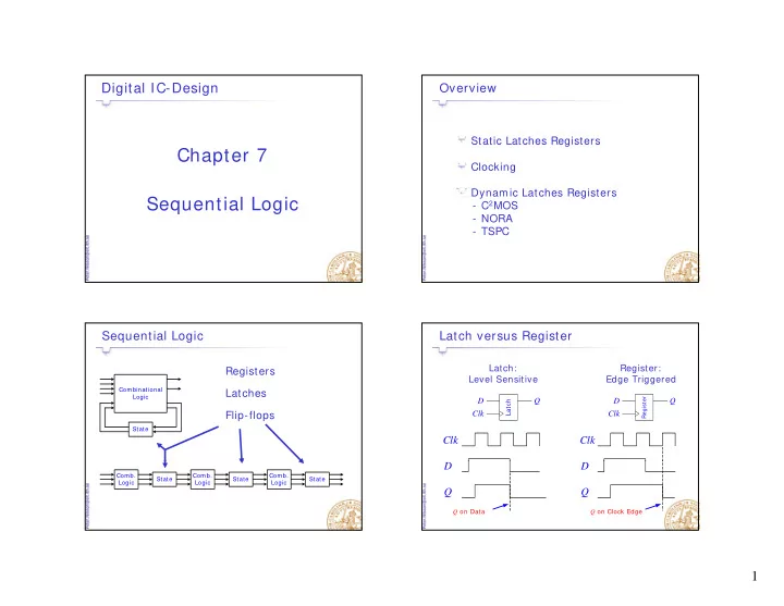
chapter 7
play

Chapter 7 Clocking Dynamic Latches Registers Sequential Logic q - PowerPoint PPT Presentation

Digital IC-Design Overview Static Latches Registers Static Latches Registers Chapter 7 Clocking Dynamic Latches Registers Sequential Logic q g - C 2 MOS - NORA - TSPC Sequential Logic Latch versus Register Latch: Register: Registers


  1. Digital IC-Design Overview Static Latches Registers Static Latches Registers Chapter 7 Clocking Dynamic Latches Registers Sequential Logic q g - C 2 MOS - NORA - TSPC Sequential Logic Latch versus Register Latch: Register: Registers Level Sensitive Edge Triggered Combinational Latches Latches Logic Register D Q D Q Latch Flip-flops Clk Clk State Clk Clk D D Comb. Comb. Comb. State State State Logic Logic Logic Q Q Q on Data Q on Clock Edge 1

  2. Clock Non-Idealities Clock Non-Idealities Both skew and jitter affects the cycle time Clock skew Skew might lead to race through the registers Spatial a iation in tempo all eq i alent Spatial variation in temporally equivalent clock edges Clock jitter Same clock Temporal variations in consecutive edges of at two the clock signal the clock signal different parts of the chip t skew t jitter Clock Non-Idealities - Feedthrough Example – Clock System V DD (Always on) V DD Global Φ Clock feedthrough Module 1 Clock 2,5 N = × f f Q SYS CLK A M Enable 2 System f Data Clock CLK Phase 1,5 Module 2 De- Locked B skew Φ Loop Q Local 0,5 Clock C Signals Enable 3 N N M Φ Module 3 -0,5 0 0,5 1 Time, ns Clock feedthrough On-Chip Clock Clock Clocked Coupling in dynamic devices Generation Gating Modules can lift the output 2

  3. Latches – Cells with Memory Latches Positive Feedback S SR-latch (00 not allowed) Static Q Dynamic Dynamic JK-latch (all inputs allowed) JK latch (all inputs allowed) CLK CLK Q Often in DSP ASICs with R "0" continuous “refresh” "1" D-latch most important in CMOS sequential Circuits. D Q CLK CLK D-latch realized with a D-latch realized with a relatively small number of Q "1" transistors "0" Capacitive Storage Static Latch 1 Static Latch 2 Weak inv. φ D Q Positive Feedback φ Q φ φ φ 8 Transistor D Q φ Weak inv. D-latch using 8 Transistor Q weak devices D-latch using φ transmission φ φ φ D Q gates φ φ D Q φ Q Q 3

  4. φ Static Latch 3 SRAM Cell (Cross-Coupled Inverters) Word Select D Q φ φ Q Q 10 Transistor φ D-latch using φ clocked inverters inverters φ φ D Q φ Q Q Q Open during read/ write Dynamic Latches Charge Sharing φ Good Design D Q φ D-latch using φ D Q φ φ Charge sharing Charge sharing Q capacitor storage capacitor storage when the inner Q transistors switch The parasitic φ φ capacitance is Q D Q φ φ often enough D Q D φ Q φ Q Discharged during high Φ 4

  5. Race Problem Register: Master-Slave Latches X D=1 D Q D Q Q φ 1 φ φ φ φ φ D D Q Q φ The Master- Signal race Q φ 2 Slave register when the is not signal latch is open φ 1 Q transparent φ 2 φ X Q Testing the Functionality of the Logic Serial Scan-based Test – Two Modes Scan in A long pipelined chain with combinatorial logic (serial) An enormous amount of test vectors will be needed Parallel Parallel Feedback makes the problem even worse in N N N N N N out Combina- Combina- Register Register Register tional tional Combina- Combina- egister egister egister tional tional Scan out Re Re Re (serial) Normal mode - N -bit wide registers Test patterns in parallel ? Scan mode - serial shift registers 5

  6. Scan Register Based Test Serial-Parallel Register Serial In Serial Out IN0 IN1 IN2 IN3 Test Test Test Test Test Test Test Test MUX or Pass REG REG Scan Scan C ll Cell C ll Cell Out In Transistors Latch Latch Latch Latch Combinational Logic Parallel Output Parallel I nput OUT0 OUT1 OUT2 OUT3 Normal mode = normal REG REG Parallel Cell Cell = scan TEST N cycles 1 cycle C Scan mode d Φ1 Serial and REG REG Parallel Cell Cell Φ2 Scan chain of N clock cycles in test sequence Scan Register Based Test Scan Test in a Datapath 1 cycle to N serial cycles N serial cycles evaluate logic A B SCANIN REG[1] REG[0] REG[2] REG[3] REG REG REG REG REG REG Cell Cell Cell Cell Cell Cell mbinational Logic mbinational Logic mbinational Logic + REG[4] REG REG REG REG REG REG Cell Cell Cell Cell Cell Cell COMPIN Partial Scan Partial Scan Com Com Com COMP SCANOUT REG REG REG REG REG REG REG[5] Cell Cell Cell Cell Cell Cell OUT 6

  7. Clocking Two-Phase Clocking Non-overlapping Overlapping True single phase clocking (TSPC) φ 1 0 0 Two phase Ext. 1 φ 2 CLK 1 Ext. Pseudo four phase, safe and slow CLK 0 φ 1 1 φ 2 0 1 Overlapping Overlapping φ 1 φ φ 1 φ Non-overlapping φ 2 φ 2 Non-overlap Overlap Pseudo Four-Phase Clocking Single-Phase Clocking Safe and Slow Two phases but only one clock wire L Large Clock Bus ge Clo k B φ 1 Cell Cell Cell Cell φ 1 Ext. φ 2 (Reg) (Reg) (Reg) (Reg) φ 1 CLK φ 2 φ φ φ φ φ φ φ φ φ φ φ φ φ φ φ φ φ 1 φ 2 φ 2 φ 2 Clock Wire 7

  8. Dynamic Register: C 2 MOS Static Registers φ 1 φ 2 φ 1 φ φ φ 2 φ 1 φ 2 φ φ D Q φ 1 φ 2 Four In Out clock φ φ φ 1 φ 2 p phases D Q φ 1 φ 2 C 2 MOS: Pipelining C 2 MOS: Overlapping Clock φ φ φ φ Closed In=1 In=0 φ φ φ Out Out Out Out Non- Non- φ φ φ φ Closed In inverting inverting Out φ φ logic φ logic φ φ φ φ Overlapping clock allowed if non-inverting logic Transparent register if inverting logic 8

  9. C 2 MOS: Overlapping Clock NORA (NO RAce) Combinational Latch Combinational Latch Closed φ φ φ φ Closed φ φ φ φ φ φ In=1 In=0 Out Out φ φ φ φ PUN PUN Closed PDN φ PDN φ Closed φ φ φ φ φ φ φ φ φ Module: Precharge on φ =0 φ Module: Precharge on φ =1 φ φ Combines np -logic and C 2 MOS True Single Phase Clocking (TSPC) True Single Phase Clocking (TSPC) N-Block P-Block N-Block P-Block φ φ Out N In φ φ φ φ Out P φ PUN Out N From φ PDN To P-Blocks N-Blocks φ φ φ φ φ φ φ φ φ Out N φ From other In N-Blocks Out P φ φ 9

  10. TSPC Reliability TSPC Reliability N P N P The clock edge must be φ φ φ φ φ φ φ φ sharp to avoid transparency sharp to avoid transparency Out N In Out N Out N X X In I φ φ Out P when the signal comes from the previous block CLK φ φ N P N P φ φ φ φ OK OK φ φ φ φ φ φ φ φ Out N In In In Out P Both N-MOS are conducting X X CLK 10

Download Presentation
Download Policy: The content available on the website is offered to you 'AS IS' for your personal information and use only. It cannot be commercialized, licensed, or distributed on other websites without prior consent from the author. To download a presentation, simply click this link. If you encounter any difficulties during the download process, it's possible that the publisher has removed the file from their server.

Recommend


More recommend