issues in fpga technologies
play

Issues%in%FPGA%Technologies Complexity%of%Logic%Element - PDF document

Issues%in%FPGA%Technologies Complexity%of%Logic%Element How%many%inputs/outputs%for%the%logic%element? Does%the%basic%logic%element%contain%a%FF?%What% type? Interconnect


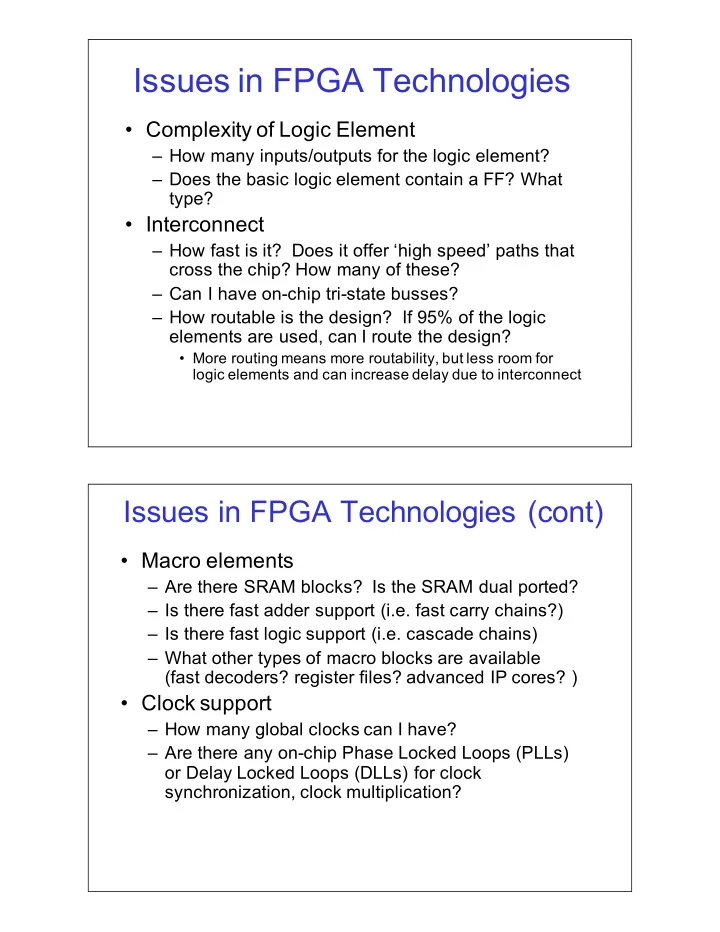
  1. Issues%in%FPGA%Technologies • Complexity%of%Logic%Element – How%many%inputs/outputs%for%the%logic%element? – Does%the%basic%logic%element%contain%a%FF?%What% type? • Interconnect – How%fast%is%it?%%Does%it%offer%‘high%speed’%paths%that% cross%the%chip?%How%many%of%these? – Can%I%have%onJchip%triJstate%busses? – How%routable%is%the%design?%%If%95%%of%the%logic% elements%are%used,%can%I%route%the%design? • More%routing%means%more%routability,%but%less%room%for% logic%elements%and%can%increase%delay%due%to%interconnect Issues%in%FPGA%Technologies%(cont) • Macro%elements – Are%there%SRAM%blocks?%%Is%the%SRAM%dual%ported?% – Is%there%fast%adder%support%(i.e.%fast%carry%chains?) – Is%there%fast%logic%support%(i.e.%cascade%chains) – What%other%types%of%macro%blocks%are%available% (fast%decoders?%register%files?%advanced%IP%cores?%) • Clock%support – How%many%global%clocks%can%I%have? – Are%there%any%onJchip%Phase%Locked%Loops%(PLLs)% or%Delay%Locked%Loops%(DLLs)%for%clock% synchronization,%clock%multiplication?
  2. Issues%in%FPGA%Technologies%(cont) • What%type%of%IO%support%do%I%have? – TTL,%CMOS,%etc – Support%for%mixed%5V,%3.3V%%IOs? • 3.3V%internal,%but%5V%tolerant%inputs? – Support%for%other%low%voltage%signaling%standards? • GTL+,%GTL%(Gunning%Transceiver%Logic)%– as%used%on% Pentium%II • HSTL%J High%Speed%Transceiver%Logic • SSTL%J Stub%SeriesJTerminate%Logic • USB%%J IO%used%for%Universal%Serial%Bus%(differential% signaling) • AGP%%J IO%used%for%Advanced%Graphics%Port – Maximum%number%of%IO?%%Package%types? • Ball%Grid%Array%(BGA)%for%high%density%IO CPLDs%and%FPGAs CPLD FPGA Complex3Programmable3Logic3Device Field/Programmable3Gate3Array Architecture PAL/like Gate3array/like Density Low/to/medium Medium/to/high Up3to316322V10s 1K3to3125K3logic3gates Performance Predictable3timing Application3dependent Over31003MHz High/performance Interconnect “Crossbar” Incremental NOTE:&First&generation&programmable&devices&(PROMs,&PALS, PLAs,&GPLAs)&Analogous&to&2Dlevel&Logic&while&CPLDs/FPGAs (programmable&interconnects)&Analogous&to&MultiDlevel&Logic

  3. Programmable%Logic%Resources 1)%Configurable%Logic%Blocks%(CLBs)%or%Logic%Elements%(LEs) J Memory%lookup%tables J ANDJOR%planes J Simple%gates 2)%%Input%/%Output%Blocks%(IOBs) J Bidirectional J Latches,%inverters,%pullup/down 3)%Interconnect%or%Routing J Local%and%global%routing%balance J Delay%and%area Each&of&these&three&Basic&Resources&Require& a&Programmable&Circuit Programming%Technologies 1)%Bipolar%fusible%link%(not%commonly%used%in%modern%devices) J Closed%device,%burned%open%by%high%current J Smallest%AreaJmore%complicated%to%fabricate J One%Time%Programmable%(OTP) 2)%Antifuse J Open%device,%closes%with%high%voltage J Small%area%but%high%voltage%required J One%Time%Programmable%(OTP) 3)%SRAM%based J Uses%pass%transistor%controlled%SRAM%cell J Large%Area J Volatile%(Reprogrammable) 4)%E/EEPROM/Flash%based J Moderate%Area J NonJVolatile%(Reprogrammed)

  4. Metal%to%Metal%Antifuse%Technology Metal%to%Metal%Antifuse%Technology

  5. Antifuse%Technology Actel%Programmable%Low%Impedance%Circuit%Element%(PLICE) Initial%“Open”% Antifuse%is%“Blown” Connection Conducting • ONO%(oxide%nitride%oxide)%Dielectric%insulates% diffusion%and%poly • ONO%“melted”%by%applying%16V%pulse%across%it *Sources&Hauck&(IEEE&Proc.),&Actel&Data&Sheets&1994 ONO%Antifuse%Technology (unprogrammed)

  6. ONO%Antifuse%Technology (programmed) E/EEPROM%Technology • Floating%Gate%%(FG)is%Completely%Isolated • Unprogrammed%Transistor%has%no%Charge%on%FG%Operates Normal%NMOS%Transistor%using%Access%Gate%(AG)%as%gate • Programmed%by%High%Voltage%on%AG%and%Low% Voltage%on%Drain%Causing%Neg.%Charge%on%Floating%Gate • Source%to%Drain%Path%cannot%be%closed%when%programmed • EPROM%uses%UV%light%to%Discharge%FG%and%erase • EEPROM%uses%high%voltages%similar%to%programming%but opposite%polarity%to%erase *Source&Hauck&(IEEE&Proc.)

  7. SRAM%Technology Can%Connect%to Pass%Transistor WEAK Allowing%Cell to%Function Similar%to% Antifuse • Pass%Transistor%is%“on”%During%Programming%and%“off”%During Normal%Operation%of%Programmed%FPGA • Inverter%Pair%Latches%Logic%Value%using%the%Upper%“weak” Keeper%Inverter • Larger%Area%than%E/EEPROM%Based%Cell • More%Easily%Reprogrammed%J Useful%for%Reconfiguration%and Prototyping • “Read”%Function%used%for%Debugging%to%Output%Programmed Configuration *Source&Hauck&(IEEE&Proc.),&Xilinx&1994,&Compton SRAM%Technology Q%or%Q’%Output NMOS%Pass from%1Jbit%SRAM Transistor Cell *Source&Hauck&(IEEE&Proc.),&Xilinx&1994,&Compton

  8. LE/CLB%Structures • Different%Styles%of%Internal%Structure – LookJUp%Tables%(LUTs) – PLA/PALJbased%Macrocells – Arrays%of%Multiplexers • Granularity%Variations • Delay%Characteristics • Internal%Programming%Technology • Scalability%J Logic%Clusters Generic%LookJUp%Table%(LUT) 0 1 2 3 4 5 6 7 *Source&Compton

  9. Registered/ByJPass%Programmable% Circuit BYPASS%bit%is%Programmed *Source&Compton Generic%LUTJBased%LE *Source&Compton

  10. Xilinx%6200%Logic%Element • Can%Compute%any%2Jinput%and%some%3Jinput%functions • Extremely%FineJgrained • Based%on%Multiplexers *Source&Compton Increasing%Granularity *Source&Compton

  11. Xilinx%4000%Series%CLB • 3%function%generators C1 C2 C3 C4 • CLB%inputs – F1JF4%to%F H13DIN3S/R3EC333 – G1JG4%to%G S/R Control G4 – H1%(&%F,%G)%to%H G DIN G3 SD YQ F' Func. • 4%CLB%outputs D Q G2 G' Gen. H' G1 – F,%G,%or%H EC RD – and%registered 1 H Y G' Func. H' Gen. S/R Control F4 F F3 Func. DIN SD XQ F2 Gen. F' D Q G' F1 H' EC RD 1 X H' F' K More&Detail&on&Next&Slide Xilinx%4000%Series%CLB

  12. Altera%Flex10k%Logic%Element Altera%Stratix%Logic%Element

  13. Xilinx%Coolrunner%EEPROM/Flash%LE Altera%Max%7000%Macrocell LAB@Local@Array This@respresents@a multiplexer Parallel@Logic controlled@by@the Expanders configuration (from@other program macrocells) Global Global Programmable Clear Clock Register To@I/O Control Block PRN Product( D Q Term Select Clock/ Matrix ENA Enable Select CLRN Clear VCC Select To@PIA Shared@Logic Expanders 36@Signals 16@Expander from@PIA Product

  14. Device%Architectures • Proportion%of%Interconnect%Resources% Versus%Logic%Elements • Routability%Among%Logic%Elements • Dedicated%Interconnections%Among%Logic% Elements • Granularity • Hierarchical%versus%Flat%Interconnections Routing%Architectures Symmetrical Routing%Matrix Row%Based Sea%of%Gates

  15. Conceptual%Diagram%of%IslandJstyle% Architecture Logic Block I/O Cells Interconnection Resources Xilinx%4000%Series%Architecture Vcc Slew Passive Rate Pull4Up, Control Pull4Down CLB CLB D""""Q Switch Output Pad" Matrix Buffer Input Buffer Q""""D CLB CLB Delay Programmable I/O3Blocks3(IOBs) Interconnect C1 C2 C3 C4 ..H1.DIN.S/R.EC... S/R Control G4 G DIN G3 SD Func. F' D Q G2 G' Gen. H' G1 EC RD 1 H Y G' Func. H' Gen. S/R F4 Control F Configurable F3 Func. DIN SD F2 Gen. F' D Q G' F1 H' Logic3Blocks3(CLBs) EC RD 1 X H' ..K F'

  16. ActelJlike%RowJbased%Architecture Logic&Module Horizontal& Track Anti6fuse Vertical& Track Altera%Flex10k%Architecture

  17. Altera%Flex10k%Architecture • Hierarchical%Interconnection%Among%Logic% Elements • Logic%Arrays%consist%of%8%Logic%Elements • Each%Embedded%Array%Block%(EAB)%has%2K% bits%of%storage • Architecturally%in%center%of%device • LA%and%EAB%connect%to%surrounding% channel%interconnect Inside%the%EAB%J Altera

  18. Altera%Stratix%Logic%Array%Blocks%(Clusters) Interconnect%Structures • Programmable%Interconnects%Generally% Dominant%Factor%in%Area%and%Delay • Composed%of%Drivers%on%Wires%and%Switch% Blocks • Bidirectional%Allow%Signal%Flow%in%Either% Direction • Directional%Allow%Signal%Flow%in%One%Direction% Only • Routing%Accomplished%via%Switch%Block%and% Driver%Programming%Bits

  19. Bidirectional%and%Directional% Interconnects *Lemieux et al., ICFPT 2004 Interconnect%Switch%Blocks Logic Element Switch%Blocks Horizontal%and%Vertical%Crossings%Represent% Programmable%Switch%Blocks *Lemieux et al., ICFPT 2004

  20. Bidirectional%Switch%Block Programmable%SingleJbit%Cells *Lemieux et al., ICFPT 2004 Directional%and%Bidirectional%Switch%Blocks *Lemieux et al., ICFPT 2004

  21. Commercial%Trends%CircaJ2000 !FPGA!MARKET!SHARE!(2000) Flash%and%Antifuse FPGA Actel Other 6% ≈ 10%% 8% Xilinx Lattice 38% 14% Altera SRAM 34% FPGA ≈ 90%% •Three%main%types:%Antifuse,%Flash,%SRAM Altera%FPGA%Family%Examples • Altera%Flex10K/10KE – LEs%(Logic%elements)%have%4Jinput%LUTS%(lookJup% tables)%+1%FF – Fast%Carry%Chain%between%LE’s,%Cascade%chain%for% logic%operations – Large%blocks%of%SRAM%available%as%well • Altera%Max7000/Max7000A – EEPROM%based,%very%fast%(Tpd%=%7.5%ns) – Basically%a%PLD%architecture%with%programmable% interconnect.%(CPLD) – Max%7000A%family%is%3.3%v

Download Presentation
Download Policy: The content available on the website is offered to you 'AS IS' for your personal information and use only. It cannot be commercialized, licensed, or distributed on other websites without prior consent from the author. To download a presentation, simply click this link. If you encounter any difficulties during the download process, it's possible that the publisher has removed the file from their server.

Recommend


More recommend