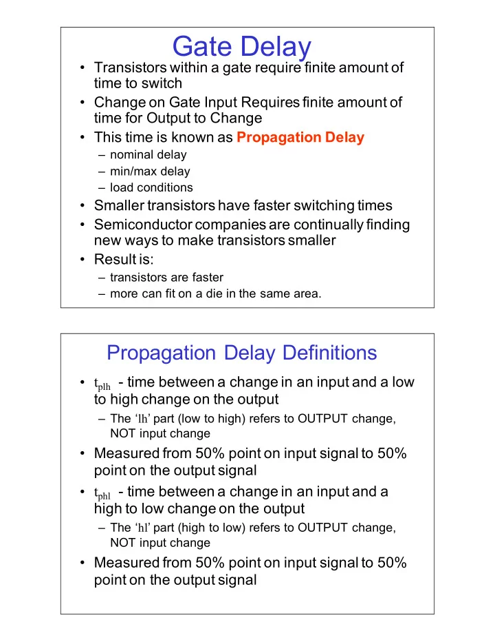
Gate%Delay Transistors%within%a%gate%require%finite%amount%of% - - PDF document

gate lay
SMART_READER_LITE
LIVE PREVIEW

Gate%Delay Transistors%within%a%gate%require%finite%amount%of% - - PDF document

Gate%Delay Transistors%within%a%gate%require%finite%amount%of% time%to%switch%% Change%on%Gate%Input%Requires%finite%amount%of% time%for%Output%to%Change This%time%is%known%as% Propagation*Delay nominal%delay min/max%delay


slide-1
SLIDE 1

Gate%Delay

  • Transistors%within%a%gate%require%finite%amount%of%

time%to%switch%%

  • Change%on%Gate%Input%Requires%finite%amount%of%

time%for%Output%to%Change

  • This%time%is%known%as%Propagation*Delay

– nominal%delay – min/max%delay – load%conditions

  • Smaller%transistors%have%faster%switching%times
  • Semiconductor%companies%are%continually%finding%

new%ways%to%make%transistors%smaller

  • Result%is:

– transistors%are%faster – more%can%fit%on%a%die%in%the%same%area.

Propagation%Delay%Definitions

  • tplh G time%between%a%change%in%an%input%and%a%low%

to%high%change%on%the%output

– The%‘lh’%part%(low%to%high)%refers%to%OUTPUT%change,% NOT%input%change

  • Measured%from%50%%point%on%input%signal%to%50%%

point%on%the%output%signal

  • tphl G time%between%a%change%in%an%input%and%a%

high%to%low%change%on%the%output

– The%‘hl’%part%(high%to%low)%refers%to%OUTPUT%change,% NOT%input%change

  • Measured%from%50%%point%on%input%signal%to%50%%

point%on%the%output%signal

slide-2
SLIDE 2

A Y

Propagation%Delay%%(non%inverting)

B Each%Input%to%Output%path%has%its%own%delay: A2Ytplh, A2Ytphl, B2Ytplh, B2Ytphl These%delays%can%be%different For%simplicity,%may%just%assign%one%delay%for%entire%gate: Ytpd Databooks%give%typical%and%maximum%propagation%delays% for%combinational%outputs A A Y H L Y H L tplh tphl

Propagation%Delay%%(non%inverting)

B

slide-3
SLIDE 3

A A Y H L Y H L tphl tplh

Propagation%Delay%%(inverting)

Signal%rise%time Signal%fall%time H L trise tfall

Rise/Fall%Time

Signal%rise%time Signal%fall%time 90% 10% 90% 10%

  • Time%from%10%%of%Steady%State%Value%to%90%%
  • f%Steady%State%Value
  • Sometimes%20G80%%Thresholds%used
slide-4
SLIDE 4

DFF%Timing

  • Propagation%Delay

– tC2Q:%%%Q%will%change%some%propagation% delay%after%change%in%C.%%Value%of%Q%is% based%on%D%input%for%DFF. – tS2Q,%tR2Q:%%Q%will%change%some% propagation%delay%after%change%on%S% input,%R%input – Note%that%there%is%NO%propagation%delay% tD2Q for%DFF! – D%is%a%Synchronous%INPUT,%no%prop% delay%value%for%synchronous%inputs D Q C S R

Setup,%Hold%Times

  • Synchronous%inputs%(e.g.%%D)%%have%

Setup,%Hold%time%specification%with% respect%to%the%CLOCK%input

  • Setup%Time:%%the%amount%of%time%the%

synchronous%input%(D)%must%be%stable before the%active%edge%of%clock

  • Hold%Time:%the%amount%of%time%the%

synchronous%input%(D)%must%be%stable* after the%active%edge%of%clock.

slide-5
SLIDE 5

Setup,%Hold%Time

tsu thd

Clock D%%changing Stable If%changes%on%D%input%violate%either%setup%or%hold%time,% then%correct%FF%operation%is%not%guaranteed% (metastability). Setup/Hold%measured%around%active%clock%edge D%%changing

Sequential%System%Timing

Combinational Logic Circuit DFF n m k k k/bit Present*State Values k/bit Next*State Values

Question:%What%is%the%MAXIMUM%frequency%of%operation%

  • f%this%system?

D Q clock

Maximum%Frequency%=%%1/%(longest%delay%path) What*are*longest*paths???

slide-6
SLIDE 6

Longest%Delay%Paths%in% Sequential%System%Diagram

Three%types%of%Paths%to%check: A.%%%%Clock%to%Output%delay:%%%Tc2q + Tcomb_Q2O_max Tcomb_Q2O is%longest%path%from%Q output%to%any%output B.%%%Register%to%Register%delay:%Tc2q + Tcomb_Q2D_max + Tsetup.%%Tcomb_Q2D is%longest%path%from%Q%dff%output%to%D%dff% input C.%%%Pin%to%Pin%combinational%delay:%%Tcomb_I2O_max (input%pin%to%output%pin,%no%intervening%registers)

Typically,%paths%of%type%“B”%are%the%worst%cases.

Inputs/Outputs%Registered

Very%often,%all%inputs%and%outputs%are%registered.%%Then% registerGtoGregister%delay%will%almost%always%determine% maximum%frequency. D Q C N Combinational% Logic Tpd_max N D Q C K K Tc2q Tsetup delay = Tc2q + Tpd_max + Tsetup

slide-7
SLIDE 7

Hold%Time%and%Shortest%Paths

D Q C N Combinational% Logic Tpd_min N D Q C K K Tc2q Thold To%satisfy%hold%time: Tc2q + Tpd_min >= Thold This%is%normally%easily%satisfied%in%a%sequential%%system.

Toggle%Frequency

D Q C toggle frequency = 1 /(Tc2q + Tsetup) assume%wire%delay%is%negligible What%about%setup%time? Tc2q + Tpd_min >= Thold Tc2q > Thold assuming%zero%wire%delay

slide-8
SLIDE 8

Setup,%Hold%Time%for%External%Inputs

External%inputs%are%buffered%through%pad%drivers%and%may%go% through%combinational%logic%before%they%reach%a%synchronous% input.%%This%buffering%adds%propagation%delay.%%How%does%this% propagation%delay%affect%the%EXTERNAL%setup%and%hold% time???? D Q C Comb Log Comb Log DIN CLK Y Thd, Tsu Thd, Tsu What%is Thd, Tsu for DIN? It%is%NOT%the%same%as%for Thd, Tsu of%the%internal%DFF!!!!!!! Thd, Tsu for%DIN is% specified%in%the%DATASHEET%for%design. ASIC%

  • r%

FPGA

External%Setup%times

Ext_su = Tsu + Tpd_DIN_max - Tpd_CLK_min worst%case Ext_su = Tsu + Tpd_DIN - Tpd_CLK

slide-9
SLIDE 9

Calculating%External%Setup%times

D Q C Comb Log Comb Log DIN CLK Tsu ASIC Worst%case%setup%time%for%DIN occurs%when%%‘DIN’%is% DELAYED relative%to%CLK.%%%Means%clock%edge%arrives%early,% requiring%DIN to%be%ready%sooner. Tpd_DIN Tpd_Clk Ext_su = Tsu + Tpd_DIN_max - Tpd_CLK_min

External%Hold%times

Ext_hd = Thd + Tpd_CLK_max - Tpd_DIN_min Ext_hd = Thd + Tpd_CLK - Tpd_DIN worst%case

slide-10
SLIDE 10

Calculating%External%Hold%times

Worst%case%hold%time%for DIN occurs%when ‘CLK’ is DELAYED relative%to DIN. Means%clock%edge%arrives%late,% requiring DIN to%hold%its%value%longer. Ext_hd = Thd + Tpd_CLK_max - Tpd_DIN_min D Q C Comb Log Comb Log DIN CLK Thd ASIC Tpd_DIN Tpd_Clk

A%Timing%Example

D Q C Q C Y A D CK U1 U2 2 ns 1 ns 8 ns 9 ns 6 ns 7 ns DFFs : Tsu = 3 ns Thd = 4 ns Tc2q = 5 ns U3 U4 U5 U6 U7 U8

slide-11
SLIDE 11

Timings

Max%Register%to%Register%Delay: = U2_Tc2q + U3_Tpd + U1_Tsu = 5 + 8 + 3 = 16 ns A_setup_time = Tsu + A2D_Tpd max - Clk_Tpd_min = Tsu + (U3_Tpd + U7_Tpd) - U8_Tpd = 3 + (8 + 1) - 2 = 10 ns A_hold_time = Thd + Clk_Tpd_max - A2D_Tpd_min = Thd + U8_Tpd - (U4_Tpd + U7_Tpd) = 4 + 2 - (7 + 1) = -2 ns

Timings%(Cont)

Clock%to%Out: = U8 Tpd + U2 Tc2q + U5 Tpd + U6 Tpd = 2 + 5 + 9 + 6 = 22 ns Pin%to%Pin%Combinational%Delay%(A2Y): = U7_Tpd + U5_Tpd + U6_Tpd = 1 + 9 + 6 = 16 ns Max Clock Freq = 1/ Max(Reg2reg, Clk2Out, Pin2Pin) = 1/ Max(16, 22, 16) = 1/ Max(16, 22, 16) = 45.5 Mhz

slide-12
SLIDE 12

DataSheet

Parameter Description Min Max Units Tclk Clock Period 22 ns Fclk Clock Frequency 45.5 MHz Atsu A setup time 10 ns Athd A hold time

  • 2

ns A2Y A to Y Tpd 16 ns Ck2Y Clock to Y tpd 22 ns

Negative%hold%times%are%typically%specified%as%0%ns

How%do%we%improve%timings?

CL CL REG U2 CL REG U1 CL

slide-13
SLIDE 13

How%do%we%improve%timings?

Add%Registers! D Q C Q C Y A D CK U1 U2 2 ns 1 ns 8 ns 9 ns 6 ns 7 ns DFFs : Tsu = 3 ns Thd = 4 ns Tc2q = 5 ns U3 U4 U5 U6 U7 U8 U9, DFF U10, DFF

New%Timings

A setup time = Tsu + A2D_Tpd_max - Clk_Tpd_min A hold time = Thd + Clk_Tpd_max - A2D_Tpd_min Max%Register%to%Register%Delay U2_Tc2q + U5_Tpd + U10_Tsu = 5 + 9 + 3 = 17 ns

slide-14
SLIDE 14

New%Timings

A setup time = Tsu + A2D_Tpd_max - Clk_Tpd_min = Tsu + (U7_Tpd) - U8_Tpd = 3 + (1) - 2 = 2 ns A hold time = Thd + Clk_Tpd_max - A2D_Tpd_min = Thd + U8_Tpd - (U7_Tpd) = 4 + 2 - ( 1) = 5 ns Max%Register%to%Register%Delay U2_Tc2q + U5_Tpd + U10_Tsu = 5 + 9 + 3 = 17 ns

New%DataSheet

Parameter Description Min Max Units Tclk Clock Period 17 ns Fclk Clock Frequency 58.8 MHz Atsu A setup time 2 ns Athd A hold time 5 ns Ck2Y Clock to Y tpd 13 ns

Most%designs%have%all%inputs,%outputs%registered.

slide-15
SLIDE 15

How%do%we%improve%timings?

CL CL REG U2 CL REG U1 CL REG REG

How%does%a%PLL/DLL%help?

  • A%Phased%Locked%Loop%or%Delay%Locked%Loop%

circuit%is%used%to%align%the%external%clock%edge% at%the%pin%with%the%internal%clock%edges%at%the% DFF%clk%pins

– Some%clock%skew%due%to%clock%routing%network%from% PLL%will%still%be%present,%but%input%buffer%delay% eliminated.

  • PLLs%and%DLLs%differ%but%we%will%consider%

them%the%same%for%this%course

  • This%means%that%we%can%drop%out%the%Clk_Tpd

term%from%the%equations

  • How%does%this%change%things?
slide-16
SLIDE 16

DLL%Example Without%PLL

ExtCK ExtCK IO Buffer Delay Q C D Q C D IntCK IntCK Buffer%Delay%(and%routing)%

slide-17
SLIDE 17

With%PLL

ExtCK ExtCK IO Buffer Delay Q C D Q C D IntCK IntCK Buffer%Delay%eliminated P L L

New%Timings%(PLL,%Inputs/Outputs%Reg)

A setup time = Tsu + A2D_Tpd_max - Clk_Tpd_min = Tsu + (U7_Tpd) - 0 (due to PLL) = 3 + (1) - 0 = 4 ns A hold time = Thd + Clk_Tpd_max - A2D_Tpd_min = Thd + 0 (due to PLL) - (U7_Tpd) = 4 + 0 - ( 1) = 3 ns Max%Register%to%Register%Delay: U2_Tc2q + U5_Tpd + U9_Tsu = 5 + 9 + 3 = 17 ns

slide-18
SLIDE 18

New%Timings%(PLL,%Inputs/Outputs%Reg)

Clock%to%Out: = U8_Tpd + U9_Tc2q + U6_Tpd = 0 (due to PLL) + 5 + 6 = 11 ns

NO%pin%to%Pin%combinational%delay!%%All%inputs/outputs% registered!

Max Clock Freq = 1/ Max(Reg2reg, Clk2Out, Pin2Pin) = 1/ Max(17, 11, 0) = 58.8 MHz

New%DataSheet%(PLL,%Inputs/Outputs% Reg)

Parameter Description Min Max Units Tclk Clock Period 17 ns Fclk Clock Frequency 58.8 MHz Atsu A setup time 4 ns Athd A hold time 3 ns Ck2Y Clock to Y tpd 11 ns Clock to Output improved; important in multiple chip designs. External Setup/Hold times closer to setup/hold times of internal DFFs.

slide-19
SLIDE 19

Chip%to%Chip%Timing%Calculation

ASIC #1 ASIC #2 CLK Inputs Need%to%know%external%setup/hold%times%all%inputs,%clk%to%

  • ut%of%all%outputs,%all%pin%to%pin%combinational%delays.

ASIC = Application%Specific%Integrated%Circuit

Max%Register%to%Register%Delay% 2%ASIC%System

Assume%no%pin%to%pin%combinational%delays%and%that% inputs/outputs%of%both%ASICs%are%registered. For%any%outputs%from%ASIC%#1%which%are%Inputs%to%ASIC%#2%find% maximum%of%ASIC%#1%Clk%to%out%+%%ASIC#2%Setup%time. For%any%outputs%from%ASIC%#2%which%are%Inputs%to%ASIC%#1%find% maximum%of%ASIC%#2%Clk%to%out%+%%ASIC#1%Setup%time. The%maximum%of%these%two%times%will%be%the%minimum%clock% period.

slide-20
SLIDE 20

Other%Factors%that%effect%Timing

  • Voltage:%%the%higher%the%voltage,%the%faster%that%

gates%switch

  • Temperature:%the%lower%the%temperature,%the%

faster%that%gates%switch

  • Process%Technology%(transistor%gate%width).%

The%shorter%the%transistor%gate%length,%the% faster%the%transistor%will%switch%%(I.e,%%0.09μ process%versus%0.045μ process).

  • In%a%given%process%run,%may%get%fast%N%

transistors,%fast%P%transistors,%slow%N% transistors,%slow%P%transistors

Device%Characterization

  • Do%timing%analysis%on%ASICs%at%four%extreme%

corners%to%make%sure%they%meet%timing%specs% under%all%conditions

  • Fastest%Case:%%Fast%N%transistors,%Fast%P%

transistors,%%High%Vdd,%Low%temperature

  • Slowest%Case:%%Slow%N%transistors,%slow%P%

transistors,%low%Vdd,%high%temperature

  • Other%two%corners%can%vary%but%two%possible%

corners%are:

– Fast%N,%Slow%P,%%Typical%Temperature – Slow%N,%Fast%P,%%Typical%Temperature

slide-21
SLIDE 21

Speed%Grades

  • Databooks%often%list%different%speed%grades for%

a%part%at%the%same%temperature

  • Simply%test%parts%that%come%off%the%fabrication%

line%and%see%how%fast%they%are

– Divide%the%parts%into%different%speed%bins – For%three%speed%grades,%a%design%goal%might%be%to% have%20%%of%your%parts%fall%in%the%upper%bin,%%50%%in% the%middle%bin,%and%25%%in%the%lower%bin. – As%the%process%matures,%more%and%more%fabricated% parts%will%move%into%the%upper%speed%bin,%at%which% point%you%make%a%new%upper%speed%bin. – Obviously,%faster%parts%cost%more%(and%are%more% profitable)

Static%Path%Analysis

  • After%your%gate%netlist%has%been%mapped%to%the%

FPGA,%a%timing%analysis%tool%will%analyze%the% paths%in%the%design%and%compute%the%timings% we%have%discussed

  • The%timing%analyzer%takes%into%account%the%

routing%delays%in%the%physical%routing%and%the% speed%grade%of%the%part%you%have%mapped%to.

– Because%routing%can%sometimes%change%somewhat% drastically%for%even%small%changes,%often%try%run% multiple%device%mappings%to%try%to%get%a%‘good% route’.

slide-22
SLIDE 22

Static%Timing%Analysis%Reports

  • The%static%timing%analyzer%will%report%the%following%times

– Register%to%Register%delays – Setup%times%of%all%external%synchronous%inputs – Clock%to%Output%delays – Pin%to%Pin%combinational%delays

  • The%clock%to%output%delay%is%sometimes%reported%as%simply%

another%pinGtoGpin%combinational%delay

  • Static%Timing%analysis%reports%are%pessimistic%since%they%

use%worst%case%conditions%G critical%paths%with%simple%delay% models

  • Dynamic%Timing%analysis%can%be%more%accurate%but%are%

much%more%computationally%intensive

  • Many%Dynamic%Timing%Analyzers%use%Assumptions%to%

improve%runtime%that%lead%to%optimistic%delays

Critical%Path%Example

  • Assume%All%Gates%Have%Unit%Delay
  • All%Inputs%Have%Data%Ready%Time%of%0
  • Longest%Topological%Path%is%Critical%Path%in%this%Case

a b c e d y z f g

WHERE*IS*THE*CRITICAL*PATH???

slide-23
SLIDE 23

Critical%Path%– Topology%AND Logic

  • Event:%Transition%of%a%Net%from%0/1%or%1/0
  • Problem%is%No%Event%Will%Propagate%Through%Path%

{...,vd,vf,vg,...}

  • Output%of%ve Must%be%“1”%for%Event%to%Propagate%Through

Vertex%vf

  • Output%of%vg Must%be%“0”%for%Event%to%Propagate%Through

Vertex%vg

  • Impossible%so%{...,vd,vf,vg,...} is%a%FALSE%PATH
  • True%Topological%Critical%Path%is%{va,vc,vd,vf,vy}

a b c e d y z f g

Delay%Modeling%Observations

  • Some%Static%Analyzers%use%Delay%Models%Based%on%

Circuit%Topology%and%Finite%Gate%Delay%(usually%worst% case)%Only

  • More%Accurate%to%Consider%False%Paths%and%Delay%

Modeling%Using%Topology%AND Logic

  • Finding*False*Paths*Requires*Logic*Simulation (for%

more%than%one%test%vector)%or%Other%Means%of% Computation%to%do%Timing%Analysis

  • Still%an%Estimate%Since%True%Delay%Also%Depends%on%

Subsequent%Input%Signal%Changes

– eg.%Consider%3Ginput%AND%with%Input%Event%000/001 versus%Event%000/111%(unequal%settling%time)

slide-24
SLIDE 24

Timing%Accurate%Simulation

  • The%timings%extracted%by%the%Timing%analysis%tool%

(routing%delays,%gate%delays%for%a%particular% speed%grade,%etc)%are%used%in%the%simulation

  • It%may%be%tempting%to%ignore%the%delays%reported%

by%the%timing%analyzer,%and%simulate%the%design% ‘at%speed’%to%see%if%it%works.

– If%the%design%simulates%correctly,%only%means%that%it% works%for%the%particular%test%vectors%that%you%used! – Different%test%vectors%exercise%different%delay%paths%G you%must%use%test%vectors%that%exercise%the%LONGEST% paths – These%test%vectors%can%be%difficult%to%find

Functional%Simulation

  • QuartusII%Supports%Functional%Simulation
  • Can%Simulate%Logic%BEFORE%Mapping%to%Device
  • Allows%for%Debugging%your%Design%Prior
  • to%Technology%Mapping
  • Comparing%Functional%to%Timing%Simulation%

Results%can%Give%Information%Regarding:

– Device%Delay%– Timing%Violations – Appropriate%Device%Chosen