
SLIDE 1
1
1
Combinational Logic
- M. Sachdev,
- Dept. of Electrical & Computer Engineering
University of Waterloo
ECE 223 Digital Circuits and Systems
2
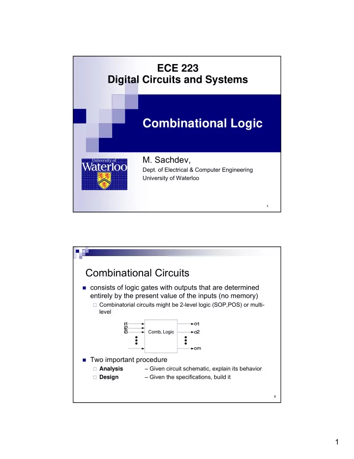
Combinational Circuits
consists of logic gates with outputs that are determined
entirely by the present value of the inputs (no memory)
Combinatorial circuits might be 2-level logic (SOP,POS) or multi-
level
Two important procedure
Analysis
– Given circuit schematic, explain its behavior
Design
– Given the specifications, build it