The CPU-Memory Gap 100,000,000.0 10,000,000.0 Disk 1,000,000.0 - - PDF document

the cpu memory gap
SMART_READER_LITE
LIVE PREVIEW

The CPU-Memory Gap 100,000,000.0 10,000,000.0 Disk 1,000,000.0 - - PDF document

High-Performance Data Storage Sean Barker 1 Data Storage Disks Hard disk (HDD) Solid state drive (SSD) Random Access Memory Dynamic RAM (DRAM) Static RAM (SRAM) Registers %rax, %rbx, ... Sean Barker 2 The


slide-1
SLIDE 1

Sean Barker

High-Performance Data Storage

1 Sean Barker

Data Storage

  • Disks
  • Hard disk (HDD)
  • Solid state drive (SSD)
  • Random Access Memory
  • Dynamic RAM (DRAM)
  • Static RAM (SRAM)
  • Registers
  • %rax, %rbx, ...

2

slide-2
SLIDE 2

Sean Barker

The CPU-Memory Gap

3

0.0 0.1 1.0 10.0 100.0 1,000.0 10,000.0 100,000.0 1,000,000.0 10,000,000.0 100,000,000.0 1985 1990 1995 2000 2003 2005 2010 2015 Time (ns) Year Disk seek time SSD access time DRAM access time SRAM access time CPU cycle time Effective CPU cycle time

DRAM CPU SSD Disk

Sean Barker

Caching

4

1 2 3 4 5 6 7 8 9 10 11 12 13 14 15 8 9 14 3

Cache Memory

Larger, slower, cheaper memory viewed as par@@oned into “blocks” Data is copied in block-sized transfer units Smaller, faster, more expensive memory caches a subset of the blocks

4 4 4 10 10 10

slide-3
SLIDE 3

Sean Barker

Cache Hit

5

1 2 3 4 5 6 7 8 9 10 11 12 13 14 15 8 9 14 3

Cache Memory

Request: 14

14

Sean Barker

Cache Miss

6

1 2 3 4 5 6 7 8 9 10 11 12 13 14 15 8 9 14 3

Cache Memory

Request: 12 Request: 12

12 12 12

slide-4
SLIDE 4

Sean Barker

Direct-Mapped Cache

7

  • Line

V D Tag Data (8 Bytes) 1 2 3 4 … … 1020 1021 1022 1023

Sean Barker

Direct-Mapped Address Components

8

  • Address division:

Line V D Tag Data (8 Bytes) 1 2 3 4 … … 1020 1021 1022 1023

Index: Which line (row) should we check? Where could data be?

Tag (19 bits) Index (10 bits) Byte offset (3 bits)

(assumes 32-bit addresses)

slide-5
SLIDE 5
  • Address division:

Line V D Tag Data (8 Bytes) 1 2 3 4 1 4217 … … 1020 1021 1022 1023

Byte offset tells us which subset of block to retrieve.

Tag (19 bits) Index (10 bits) Byte offset (3 bits) 4217 4 2

0 1 2 3 4 5 6 7

Sean Barker

Direct-Mapped Address Components

9 Sean Barker

Direct-Mapped Cache Lookup

10 V D Tag Data …

=

Tag Index Byte offset

0: miss 1: hit Select Byte(s) Data Input: Memory Address

&

slide-6
SLIDE 6

Sean Barker

2-Way Set Associative (1024 lines)

11

V D Tag Data (8 Bytes) 1 3941 … Set # V D Tag Data (8 Bytes) 1 2 3 4 1 1 4063 … … 508 509 510 511 Tag (20 bits) Set (9 bits) Byte offset (3 bits) 3941 4

Same capacity as previous example: 1024 rows with 1 entry vs. 512 rows with 2 entries

Sean Barker

2-Way Set Associative Line Matching

12

V D Tag Data (8 Bytes) 1 3941 … Set # V D Tag Data (8 Bytes) 1 2 3 4 1 1 4063 … … 508 509 510 511 Tag (20 bits) Set (9 bits) Byte offset (3 bits) 3941 4

0 1 2 3 4 5 6 7 0 1 2 3 4 5 6 7 Multiplexer Select correct value.

slide-7
SLIDE 7

Sean Barker

General Cache Model (S, E, B)

13

E = 2e lines per set S = 2s sets

0 1 2

B-1 tag

v

valid bit B = 2b bytes per cache block (the data)

t bits s bits b bits

Address of word: tag set index block

  • ffset

Sean Barker

Locality

14

¢ Temporal locality: ¢ Spa0al locality:

slide-8
SLIDE 8

Sean Barker

Locality Example

15

sum = 0; for (i = 0; i < n; i++) sum += a[i]; return sum;

Sean Barker

Locality Design

16

int sum_array_rows(int a[M][N]) { int i, j, sum = 0; for (i = 0; i < M; i++) for (j = 0; j < N; j++) sum += a[i][j]; return sum; } int sum_array_cols(int a[M][N]) { int i, j, sum = 0; for (j = 0; j < N; j++) for (i = 0; i < M; i++) sum += a[i][j]; return sum; }

(v1) (v2)

slide-9
SLIDE 9

Sean Barker

Intel Core i7 Cache Hierarchy

17

Regs L1 d-cache L1 i-cache L2 unified cache Core 0 Regs L1 d-cache L1 i-cache L2 unified cache Core 3

L3 unified cache (shared by all cores) Main memory Processor package L1 i-cache and d-cache: 32 KB, 8-way, Access: 4 cycles L2 unified cache: 256 KB, 8-way, Access: 10 cycles L3 unified cache: 8 MB, 16-way, Access: 40-75 cycles Block size: 64 bytes for all caches.

Sean Barker

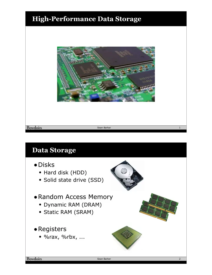
The Memory Hierarchy

18

Local secondary storage (disk)

Larger Slower Cheaper per byte

Remote secondary storage (tapes, Web servers / Internet)

~100 M cycles to access On Chip Storage

Smaller Faster Costlier per byte

Main memory (DRAM)

~100 cycles to access

CPU instrs can directly access

slower than local disk to access Registers 1 cycle to access

Cache(s) (SRAM)

~10’s of cycles to access

Flash SSD / Local network L1, L2