Cache Systems CPU Main Main CPU Memory Memory 400MHz 10MHz - - PDF document

cache systems
SMART_READER_LITE
LIVE PREVIEW

Cache Systems CPU Main Main CPU Memory Memory 400MHz 10MHz - - PDF document

Cache Systems CPU Main Main CPU Memory Memory 400MHz 10MHz Cache 10MHz Memory Hierarchy Design Bus 66MHz Bus 66MHz Chapter 5 and Appendix C Data object Block transfer transfer Main CPU Cache Memory 1 4 Example: Two-level


slide-1
SLIDE 1

1

Memory Hierarchy Design

1

Chapter 5 and Appendix C

Overview

  • Problem

– CPU vs Memory performance imbalance

  • Solution

– Driven by temporal and

2

Driven by temporal and spatial locality – Memory hierarchies

  • Fast L1, L2, L3 caches
  • Larger but slower

memories

  • Even larger but even

slower secondary storage

  • Keep most of the action in

the higher levels

Locality of Reference

  • Temporal and Spatial
  • Sequential access to memory
  • Unit-stride loop (cache lines = 256 bits)

for (i = 1; i < 100000; i++)

3

  • Non-unit stride loop (cache lines = 256 bits)

sum = sum + a[i]; for (i = 0; i <= 100000; i = i+8) sum = sum + a[i];
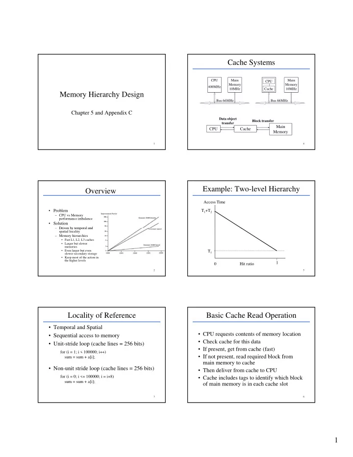
Cache Systems

CPU 400MHz Main Memory 10MHz Main Memory 10MHz Bus 66MHz Bus 66MHz CPU Cache

4

CPU Cache Main Memory

Data object transfer Block transfer

Example: Two-level Hierarchy

T1+T2 Access Time

5

1 T1 Hit ratio

Basic Cache Read Operation

  • CPU requests contents of memory location
  • Check cache for this data
  • If present, get from cache (fast)

If d i d bl k f

6

  • If not present, read required block from

main memory to cache

  • Then deliver from cache to CPU
  • Cache includes tags to identify which block
  • f main memory is in each cache slot
slide-2
SLIDE 2

2

Elements of Cache Design

  • Cache size
  • Line (block) size
  • Number of caches
  • Mapping function

7

Mapping function

– Block placement – Block identification

  • Replacement Algorithm
  • Write Policy

Cache Size

  • Cache size << main memory size
  • Small enough

– Minimize cost – Speed up access (less gates to address the cache) Keep cache on chip

8

– Keep cache on chip

  • Large enough

– Minimize average access time

  • Optimum size depends on the workload
  • Practical size?

Line Size

  • Optimum size depends on workload
  • Small blocks do not use locality of reference

principle

  • Larger blocks reduce the number of blocks

9

– Replacement overhead

  • Practical sizes?

Cache Main Memory Tag

Number of Caches

  • Increased logic density => on-chip cache

– Internal cache: level 1 (L1) – External cache: level 2 (L2)

  • Unified cache

10

– Balances the load between instruction and data fetches – Only one cache needs to be designed / implemented

  • Split caches (data and instruction)

– Pipelined, parallel architectures

Mapping Function

  • Cache lines << main memory blocks
  • Direct mapping

– Maps each block into only one possible line – (block address) MOD (number of lines)

11

  • Fully associative

– Block can be placed anywhere in the cache

  • Set associative

– Block can be placed in a restricted set of lines – (block address) MOD (number of sets in cache)

Cache Addressing

Block address Block offset Index Tag

12

Block offset – selects data object from the block Index – selects the block set Tag – used to detect a hit

slide-3
SLIDE 3

3

Direct Mapping

13

Associative Mapping

14

K-Way Set Associative Mapping

15

Replacement Algorithm

  • Simple for direct-mapped: no choice
  • Random

– Simple to build in hardware

  • LRU

16

Associativity Two-way Four-way Eight-way Size

LRU Random LRU Random LRU Random 16KB 5.18% 5.69% 4.67% 5.29% 4.39% 4.96% 64KB 1.88% 2.01% 1.54% 1.66% 1.39% 1.53% 256KB 1.15% 1.17% 1.13% 1.13% 1.12% 1.12%

Write Policy

  • Write is more complex than read

– Write and tag comparison can not proceed simultaneously – Only a portion of the line has to be updated

  • Write policies

17

Write policies

– Write through – write to the cache and memory – Write back – write only to the cache (dirty bit)

  • Write miss:

– Write allocate – load block on a write miss – No-write allocate – update directly in memory

Alpha AXP 21064 Cache

Tag Index offset 21 8 5 Address Data data In out

CPU

Valid Tag Data (256)

18

Lower level memory =? Write buffer

slide-4
SLIDE 4

4

Write Merging

Write address V V V V 100 104 108 112 1 1 1 1

19

Write address V V V V 112 100 1 1 1 1 1

DECstation 5000 Miss Rates

10 15 20 25 30 %

  • Instr. Cache

Data Cache Unified 20 5 10 1 KB 2 KB 4 KB 8 KB 16 KB 32 KB 64 KB 128 KB Cache size

Direct-mapped cache with 32-byte blocks Percentage of instruction references is 75%

Cache Performance Measures

  • Hit rate: fraction found in that level

– So high that usually talk about Miss rate – Miss rate fallacy: as MIPS to CPU performance,

  • Average memory-access time

= Hit time + Miss rate x Miss penalty (ns)

21

Hit time + Miss rate x Miss penalty (ns)

  • Miss penalty: time to replace a block from lower

level, including time to replace in CPU – access time to lower level = f(latency to lower level) – transfer time: time to transfer block =f(bandwidth)

Cache Performance Improvements

  • Average memory-access time

= Hit time + Miss rate x Miss penalty

  • Cache optimizations

– Reducing the miss rate

22

– Reducing the miss penalty – Reducing the hit time

Example

Which has the lower average memory access time: A 16-KB instruction cache with a 16-KB data cache or A 32-KB unified cache Hit time = 1 cycle Miss penalty = 50 cycles

23

p y y Load/store hit = 2 cycles on a unified cache Given: 75% of memory accesses are instruction references. Overall miss rate for split caches = 0.75*0.64% + 0.25*6.47% = 2.10% Miss rate for unified cache = 1.99% Average memory access times: Split = 0.75 * (1 + 0.0064 * 50) + 0.25 * (1 + 0.0647 * 50) = 2.05 Unified = 0.75 * (1 + 0.0199 * 50) + 0.25 * (2 + 0.0199 * 50) = 2.24

Cache Performance Equations

CPUtime = (CPU execution cycles + Mem stall cycles) * Cycle time Mem stall cycles = Mem accesses * Miss rate * Miss penalty CPUtime = IC * (CPIexecution + Mem accesses per instr * Miss rate * Miss penalty) * Cycle time

24

Misses per instr = Mem accesses per instr * Miss rate CPUtime = IC * (CPIexecution + Misses per instr * Miss penalty) * Cycle time

slide-5
SLIDE 5

5

Reducing Miss Penalty

  • Multi-level Caches
  • Critical Word First and Early Restart
  • Priority to Read Misses over Writes
  • Merging Write Buffers

25

g g

  • Victim Caches

Multi-Level Caches

  • Avg mem access time = Hit time(L1) + Miss Rate

(L1) X Miss Penalty(L1)

  • Miss Penalty (L1) = Hit Time (L2) + Miss Rate

(L2) X Miss Penalty (L2)

  • Avg mem access time = Hit Time (L1) + Miss

Rate (L1) X (Hit Time (L2) + Miss Rate (L2) X

26

( ) ( ( ) ( ) Miss Penalty (L2)

  • Local Miss Rate: number of misses in a cache

divided by the total number of accesses to the cache

  • Global Miss Rate: number of misses in a cache

divided by the total number of memory accesses generated by the cache

Performance of Multi-Level Caches

27

Critical Word First and Early Restart

  • Critical Word First: Request the missed

word first from memory

  • Early Restart: Fetch in normal order, but as

soon as the requested word arrives, send it

28

to CPU Giving Priority to Read Misses over Writes SW R3, 512(R0) LW R1, 1024 (R0) LW R2, 512 (R0)

  • Direct-mapped, write-through cache

29

pp , g mapping 512 and 1024 to the same block and a four word write buffer

  • Will R2=R3?
  • Priority for Read Miss?

Victim Caches

30

slide-6
SLIDE 6

6

Reducing Miss Rates: Types of Cache Misses

  • Compulsory

– First reference or cold start misses

  • Capacity

– Working set is too big for the cache – Fully associative caches

31

Fully associative caches

  • Conflict (collision)

– Many blocks map to the same block frame (line) – Affects

  • Set associative caches
  • Direct mapped caches

Miss Rates: Absolute and Distribution

32

Reducing the Miss Rates

  • 1. Larger block size
  • 2. Larger Caches
  • 3. Higher associativity

4 Pseudo-associative caches

33

  • 4. Pseudo associative caches
  • 5. Compiler optimizations
  • 1. Larger Block Size
  • Effects of larger block sizes

– Reduction of compulsory misses

  • Spatial locality

– Increase of miss penalty (transfer time) R d i f b f bl k

34

– Reduction of number of blocks

  • Potential increase of conflict misses
  • Latency and bandwidth of lower-level memory

– High latency and bandwidth => large block size

  • Small increase in miss penalty

Example

35

  • 2. Larger Caches
  • More blocks
  • Higher probability of getting the data
  • Longer hit time and higher cost
  • Primarily used in 2nd level caches

36

y

slide-7
SLIDE 7

7

  • 3. Higher Associativity
  • Eight-way set associative is good enough
  • 2:1 Cache Rule:

– Miss Rate of direct mapped cache size N = Miss Rate 2-way cache size N/2

37

  • Higher Associativity can increase

– Clock cycle time – Hit time for 2-way vs. 1-way external cache +10%, internal + 2%

  • 4. Pseudo-Associative Caches
  • Fast hit time of direct mapped and lower conflict

misses of 2-way set-associative cache?

  • Divide cache: on a miss, check other half of cache

to see if there, if so have a pseudo-hit (slow hit)

Hit time

38

  • Drawback:

– CPU pipeline design is hard if hit takes 1 or 2 cycles – Better for caches not tied directly to processor (L2) – Used in MIPS R1000 L2 cache, similar in UltraSPARC

Pseudo hit time Miss penalty

Pseudo Associative Cache

Address Data Data in out

CPU

Tag

Data 1 1

39

Write buffer Lower level memory

2 2 3

=? =?

  • 5. Compiler Optimizations
  • Avoid hardware changes
  • Instructions

– Profiling to look at conflicts between groups of instructions

D

40

  • Data

– Loop Interchange: change nesting of loops to access data in order stored in memory – Blocking: Improve temporal locality by accessing “blocks” of data repeatedly vs. going down whole columns or rows

Loop Interchange

/* Before */ for (j = 0; j < 100; j = j+1) for (i = 0; i < 5000; i = i+1) x[i][j] = 2 * x[i][j]; /* After */ for (i = 0; i < 5000; i = i+1) f (j j < 100 j j+1)

41

for (j = 0; j < 100; j = j+1) x[i][j] = 2 * x[i][j];

  • Sequential accesses instead of striding through

memory every 100 words; improved spatial locality

  • Same number of executed instructions

Blocking (1/2)

/* Before */ for (i = 0; i < N; i = i+1) for (j = 0; j < N; j = j+1){ r = 0; for (k = 0; k < N; k = k+1) r = r + y[i][k]*z[k][j]; x[i][j] = r; };

42

  • Two Inner Loops:

–Read all NxN elements of z[] –Read N elements of 1 row of y[] repeatedly –Write N elements of 1 row of x[]

  • Capacity Misses a function of N & Cache Size:

–3 NxNx4 => no capacity misses

–Idea: compute on BxB submatrix that fits

slide-8
SLIDE 8

8

Blocking (2/2)

/* After */ for (jj = 0; jj < N; jj = jj+B) for (kk = 0; kk < N; kk = kk+B) for (i = 0; i < N; i = i+1) for (j = jj; j < min(jj+B-1,N); j=j+1){ r = 0; for(k=kk; k<min(kk+B-1,N);k =k+1) r = r + y[i][k]*z[k][j];

43

y j x[i][j] = x[i][j] + r; };

  • B called Blocking Factor

Reducing Cache Miss Penalty or Miss Rate via Parallelism

  • 1. Nonblocking Caches
  • 2. Hardware Prefetching
  • 3. Compiler controlled Prefetching

44

  • 1. Nonblocking Cache
  • Out-of-order

execution

– Proceeds with next f h hil i i

45

fetches while waiting for data to come

  • 2. Hardware Prefetching
  • Instruction Prefetching

– Alpha 21064 fetches 2 blocks on a miss – Extra block placed in stream buffer – On miss check stream buffer

  • Works with data blocks too:

46

– 1 data stream buffer gets 25% misses from 4KB DM cache; 4 streams get 43% – For scientific programs: 8 streams got 50% to 70% of misses from 2 64KB, 4-way set associative caches

  • Prefetching relies on having extra memory

bandwidth that can be used without penalty

  • 3. Compiler-Controlled Prefetching
  • Compiler inserts data prefetch instructions

– Load data into register (HP PA-RISC loads) – Cache Prefetch: load into cache (MIPS IV, PowerPC) – Special prefetching instructions cannot cause faults; a form of speculative execution

47

  • Nonblocking cache: overlap execution with prefetch
  • Issuing Prefetch Instructions takes time

– Is cost of prefetch issues < savings in reduced misses? – Higher superscalar reduces difficulty of issue bandwidth

Reducing Hit Time

  • 1. Small and Simple Caches
  • 2. Avoiding address Translation during

Indexing of the Cache

48

slide-9
SLIDE 9

9

Small and Simple Caches

49

Avoiding Address Translation during Indexing

  • Virtual vs. Physical Cache
  • What happens when address translation is

done

  • Page offset bits to index the cache

50

g

TLB and Cache Operation

Page# Offset TLB Miss Hit Virtual address R l dd TLB Operation Cache Operation

51

Tag Remainder Cache Miss Hit Value Real address Main Memory Value Page Table

+

Main Memory Background

  • Performance of Main Memory:

– Latency: Cache Miss Penalty

  • Access Time: time between request and word arrives
  • Cycle Time: time between requests

– Bandwidth: I/O & Large Block Miss Penalty (L2)

  • Main Memory is DRAM: Dynamic Random Access Memory

– Dynamic since needs to be refreshed periodically

52

y c s ce eeds o be e es ed pe od c y – Addresses divided into 2 halves (Memory as a 2D matrix):

  • RAS or Row Access Strobe
  • CAS or Column Access Strobe
  • Cache uses SRAM: Static Random Access Memory

– No refresh (6 transistors/bit vs. 1 transistor /bit, area is 10X) – Address not divided: Full addreess

  • Size: DRAM/SRAM - 4-8

Cost & Cycle time: SRAM/DRAM - 8-16

Main Memory Organizations

CPU Cache CPU Cache CPU C h Multiplexor

Simple Wide Interleaved

53

bus Memory bus Memory bank 0 Memory bank 1 Memory bank 2 Memory bank 3 Memory Cache bus 32/64 bits 256/512 bits

sp

Interleaved Memory

54

slide-10
SLIDE 10

10

Performance

  • Timing model (word size is 32 bits)

– 1 to send address, – 6 access time, 1 to send data – Cache Block is 4 words

  • Simple M.P.

= 4 x (1+6+1) = 32

55

p ( )

  • Wide M.P.

= 1 + 6 + 1 = 8

  • Interleaved M.P. = 1 + 6 + 4x1 = 11