
SLIDE 1
Page 1
2
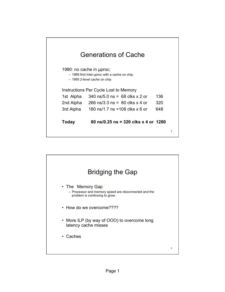
Generations of Cache
1980: no cache in µproc;
– 1989 first Intel µproc with a cache on chip. – 1995 2-level cache on chip
Instructions Per Cycle Lost to Memory 1st Alpha 340 ns/5.0 ns = 68 clks x 2 or 136 2nd Alpha 266 ns/3.3 ns = 80 clks x 4 or 320 3rd Alpha 180 ns/1.7 ns =108 clks x 6 or 648 Today 80 ns/0.25 ns = 320 clks x 4 or 1280
3
Bridging the Gap
- The “Memory Gap”
– Processor and memory speed are disconnected and the problem is continuing to grow.
- How do we overcome????
- More ILP (by way of OOO) to overcome long
latency cache misses
- Caches