
SLIDE 1
Shared Memory Bus for Multiprocessor Systems
Mat Laibowitz and Albert Chiou Group 6
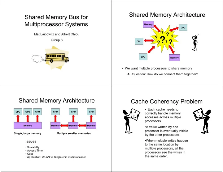
Shared Memory Architecture
CPU Memory CPU
- We want multiple processors to share memory
Question: How do we connect them together?
CPU Memory
?
?
?
?
?
? ?
?
Shared Memory Architecture
CPU CPU Memory CPU CPU Memory CPU Memory CPU Memory
Single, large memory Multiple smaller memories
Issues
- Scalability
- Access Time
- Cost
- Application: WLAN vs Single chip multiprocessor
Cache Coherency Problem
$ $ 1
- Each cache needs to
correctly handle memory accesses across multiple processors
- A value written by one
processor is eventually visible by the other processors
- When multiple writes happen