
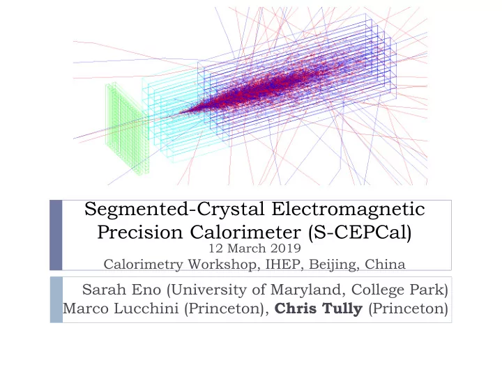
SLIDE 1
Segmented-Crystal Electromagnetic Precision Calorimeter (S-CEPCal)
Sarah Eno (University of Maryland, College Park) Marco Lucchini (Princeton), Chris Tully (Princeton)
12 March 2019
Calorimetry Workshop, IHEP, Beijing, China
Segmented-Crystal Electromagnetic Precision Calorimeter (S-CEPCal) - - PowerPoint PPT Presentation
Segmented-Crystal Electromagnetic Precision Calorimeter (S-CEPCal) 12 March 2019 Calorimetry Workshop, IHEP, Beijing, China Sarah Eno (University of Maryland, College Park) Marco Lucchini (Princeton), Chris Tully (Princeton) Performance Goals
12 March 2019
Calorimetry Workshop, IHEP, Beijing, China
} Put Zàee on equal footing with Z൵
}
x3 improvement on electron Brem. energy measurement
} Improve PFA EM shower imaging and separation
}
x100 increase on EM shower sampling fraction (1/300 à ~1)
} Incorporate Precision Time-of-Flight System
}
~20ps MIP/photon timing with high granularity (~3mm)
} Include Dual-Readout capabilities for hadrons
}
Dual wavelength filters for Cherenkov/Scint discr.
} Extend Physics Program w/ EM Res. and Timing
}
Neutrino counting (Zànng/Z൵g), Long-lived Particles, Cosmics/Out-of-time background reduction for Emiss
} Cost-effective solution
}
Segmented crystals with SiPM readout
2
3
0.5 GeV 1 GeV 10 GeV 45 GeV
counting tracks and measuring momentum here (in front of T1)
Count Tracks (e+,e-, photons) Crossing Here Tracker Material Increasing 6-Layer Silicon Tracker S-CEPCal
4
} Muons } Electrons
Muon Track Δp/p ~0.3% Electron Track Δp/p tail ~1-2% (two tracks)
5
} For EM showers in a sampling calorimeter, the energy
(Courtesy of R. Wigmans) * Si-W (300µm - HGC) * Si-W (100µm - HGC) Homogeneous crystals
X0(Si)/X0(W)=27
○
LYSO:Ce crystals
○
SiPMs
○
3x3x54 mm³ active cell
○
3x3 mm² SiPMs (15-25 um)
6 6
1 layer: 30 ps 2 layers: 20 ps + tracking
Front segment with SiPM in front and rear segment with SiPM on back à Avoids dead material at shower max
○
PbWO crystals
○
front segment 5 cm (~5.4X0)
○
rear segment for core shower
○
(15 cm ~16.3X0)
○
10x10x200 mm³ of crystal
○
5x5 mm² SiPMs (10-15 um)
< 5%/sqrt(E) (+) 1% ~30 ps timing achieved for pT>40GeV
7
1 −
10 1 10
2
10
Beam energy [GeV]
1 10
2
10
(E) / E [%]
eff
σ
total energy resolution 0.5% ⊕ E (E)/E = 5.0% /
eff
σ shower containment fluctuations photostatistics
Geant4 Simulation: Segmented Crystal Calorimeter - Electrons
8
○ FE/ASIC for read-out → PCB material ○ Cooling plate ○ Cables
○ 5 cm in front of crystal timing layer T1 (for T1 read-out) ○ 10 cm in front of crystal ECAL E1
■ 5 cm for T2 and 5 cm for E1 → cooling plate may be shared
○ 5 cm in front of crystal ECAL E2 (for E2 read-out)
○ Realistic cooling plate ~ 3 mm Al → 0.035 X0 ○ PCB ~ 2 mm, + cables, etc ○ total: 0.056 X0 (5 mm Al equivalent) for each layer ○ Scan up to 0.5X0 / layer
T1+T2 0.8X0 E1 5X0 E2 15X0
Negligible degradation up to 10 mm Al Effect more pronounced below 1 GeV
rear
9
Shower fluctuations only Total (including photostat.) Stochastic term vs dead material
10
1.2 m, 0.1-0.7 X0, Si 5 cm spacing 5 mm Al 0.056 X0 (cooling, services)
Al
130 mm
0.3λ0
Solenoid 0.5 λ0 4.5 X0 Fe
84 mm
0.5λ0 4.8X0
Fe
84 mm
0.5λ0 4.8X0
Fe
84 mm
0.5λ0 4.8X0
1λ0 1λ0 1λ0 5λ0 11 layers 4 layers 2 layers 2 layers
HCAL Segmented Crystal ECAL + Timing Tracker
T1+T2 0.8X0 E1 5X0 E2 15X0
11
12
SC-E(P)CAL
○ Realistic material budget ~0.3X0 ? ○ Scan up to 0.7X0
1.2 m, 0.1-0.7 X0, Si T1+T2 0.8X0
13
One event Several thousand events
Cooling plate e rd
14
electron
T1+T2 E1 E2
15
16
17
18
19
20
20 40 60 80 100 120
Energy deposit [GeV]
1 10
2
10
Counts
ECAL: total energy ECAL: front segment ECAL: rear segment
120 GeV electron
0.2 0.4 0.6 0.8 1
Energy deposit [GeV]
1 10
2
10
Counts
ECAL: total energy ECAL: front segment ECAL: rear segment
120 GeV pion
0.01 0.02 0.03 0.04 0.05
Energy deposit [GeV]
1 10
2
10
Counts
Timing: total energy Timing: first layer Timing: second layer
120 GeV electron
0.002 0.004 0.006 0.008 0.01
Energy deposit [GeV]
1 10
2
10
Counts
Timing: total energy Timing: first layer Timing: second layer
120 GeV pion
Timing Layers electron Calo Layers electron
Timing Layers
Calo Layers p±
21
1 −
10 1 10
2
10
Total energy deposit in ECAL [GeV]
2 −
10
1 −
10 1
Ratio ECAL front / ECAL rear
2 4 6 8 10 12
45 GeV
converting pions
non-converting pions
electrons
22
○
at LCE~2.5%, PDE ~ 20% → LY>80 ph/MeV
○
Ok for PWO (~100 ph/MeV)
○
~ 35000-70000 phe for ~72 GeV (at PDE~20-40% resp.)
○
LCE~2.5%
○
if cell size: 15 um → cells / SiPM ~110,000 and PDE up to 40%
○
if cell size: 10 um → cells / SiPM ~250,000 and PDE up to 25%
○
40 phe signal
○
Noise from SiPM within 30 ns integration gate negligible (DCR<10MHz → noise<1 phe)
23
○ for LCE~2.5% (9 mm² SiPM), PDE ~ 20% → The crystal must have a LY>80 ph/MeV
○ with SiPM area = crystal end face → LCE~30%
Crystal Scintillator (eg. BGO, LYSO…) Photodetectors (eg. FPMT, SiPM…)
1x1x40cm³
Basic Module Basic Unit
} Tiles and Bars (few mm thick w/ area of ~1cm2)
} CMS MTD: Single layer ~330,000 channels } Stereo readout for bars (L/R) ~25ps timing resolution
24
by Yuexin Wang
Similar study at IHEP
3x3x50mm3 Option A for CMS MIP Timing Detector TDR
Non-wrapped crystal bar with 2 SiPMs attached at each end
crystal
incoming particles
25
Single Layer (30 ps) Improves by 1/√2 w/Dble Layer
26
Good PDE at 600 nm
27
1.2 m, 0.1-0.7 X0, Si 5 cm spacing 5 mm Al 0.056 X0 (cooling, services)
Al
130 mm
0.3λ0
Solenoid 0.5 λ0 4.5 X0 Fe
84 mm
0.5λ0 4.8X0
Fe
84 mm
0.5λ0 4.8X0
Fe
84 mm
0.5λ0 4.8X0
1λ0 1λ0 1λ0 5λ0 11 layers 4 layers 2 layers 2 layers
HCAL Segmented Crystal ECAL + Timing Tracker
T1+T2 0.8X0 E1 5X0 E2 15X0
Sc/C filters 2x SiPM Sc/C filters 2x SiPM
Projective Sc/C Fiber Bundles?
Scint.fibers SiPM Ch.fibers SiPM
Projective or Planar Sc/C Tiles/Fiber Bundles? Muon System Plastic
Solenoid Inner Radius Outside ECAL and ECAL/HCAL Interface?
} EM Resolution also improves angular measurements
} Recoil photons (~8% of full √s collision rate)
} New Physics Searches and Neutrino Counting
28
Recoil Mass (GeV) Events / 4 GeV Data Nν = 2 Nν = 3 Nν = 4
100 200 300 400 50 100 150 200
e+e− → νν
_(γ)
Nν = 4 Nν = 2 e+e− → νν
_γ(γ)
√s
(GeV)
σ (nb)
L3
10
10
1 10 100 120 140 160 180 200
Improved Syst. (A. Blondel)
https://arxiv.org/abs/0801.1592
29
}
Zàe+e- recoil resolution w/ Brem. recovery methods
}
Highly resolved PFA clustering from high sampling fraction
}
20ps Resolution Time-of-Flight Particle ID for p/K/p
}
Photon counting with high fidelity/angular resolution
HEP crystal calorimeters
flexible, compact and lower cost solution for a high resolution ECAL
direction combined with 20 ps timing capabilities extends the physics program for particle ID, long-lived particles and improves out-of-time background rejection
30
} For HZ production, all Z recoils matter
} ~70% of Z decay are hadronic
} Particle Flow Principle
} Optimal use of measurement information applied to each
} Charged hadrons (~65%)
◻ Replaced by track (~0.1%)
} Neutral hadron (~10%)
◻ HCAL (~45%/√E)
} Photons/EM (~25%)
◻ ECAL (~15%/√E)
31
3 − 2 − 1 − 1 2 3
Energy fraction
0.1 0.2 0.3 0.4 0.5 0.6 0.7 0.8 0.9
(8 TeV)
19.7 fb
CMS
Forward EM energy Forward hadrons Leptons Neutral hadrons Photons Charged hadrons Charged PU hadrons < 74 GeV
T
56 < p R=0.5
T
Anti-k Markers: Data Histogram: MC
Data-MC (%)
4
32
○
QEVPT ~22%,
○
LCE ~ 9% (1 VPT: size~ 11 mm radius - area: 380 mm²)
○
PbWO, crystal end face size: ~30x30 mm²
○
QEAPD~75%,
○
LCE~9% (2xAPDs, size: 5x5 mm²)
○
PbWO crystal size: ~22x22 mm²
http://iopscience.iop.org/article/10.1088/1748-0221/2/04/P04004/pdf https://arxiv.org/pdf/1306.2016.pdf
PANDA ECAL PWO-II development: → factor 4 higher LO at -25°C wrt to +25°C → ~20 phe/MeV @PDE=20% → <2% stochastic term https://arxiv.org/pdf/0810.1216.pdf
} Typical dynamic range customization for SiPM
} More (small) SPADS to count more photons (50à15μm) } Bright crystal (LYSO, GAGG) and high photodetection
33
Currently: Large device ~6x6mm2 CMS MTD ~4.5 m2 of SiPMs (of 3x3mm2) Segmented Crystal ECAL: ~200 m2 of crystal surface (3-4 layers) Which SiPM device?
} Large pixel count w/ large gain leads to current
} Multiple analog outputs per device } Regional lumped analog sums - split output currents per
} Multi-gain SPADs (5, 15, 50μm) for different cell sizes and
} On-chip ADC with regional serializers } Commercial market for LIDAR advances is growing rapidly
34